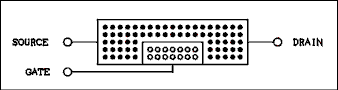
Figure 4.15 Junction Field Effect Transistor.
For a verbal description click here.
Here is another small excerpt from my textbook. See Semiconductor Diodes for details.Chapter 4.
The Field Effect Transistor.4.4 The Field Effect Transistor (FET).
There are two classes of field effect transistors, junction field effect transistors, JFETs, and metal oxide semiconductor field effect transistor, MOSFETs. We will begin with JFETs.The Junction Field Effect Transistor.
Figure 4.15 Junction Field Effect Transistor.
For a verbal description click here.
Figure 4.15 shows an N channel junction field effect transistor (JFET). If a battery is connected to the ends of the channel, (source and drain) current will flow as if it were a resistor. Like any other resistance device the resistance will depend on the length and cross-section area of the block of semiconductor material.It is the cross-section area which is important in the JFET. If the gate to channel junction is reverse-biased the depletion region will grow outward from the gate as shown in Figure 4.16. As the depletion region grows larger the conduction cross-section area is decreased. The depletion region does not conduct current. As the reverse bias voltage on the gate-channel junction is increased, the resistance of the channel is increased. At comparatively large gate to channel voltages (about 10 volts) the channel resistance is approaching infinity. At a gate to channel voltage of zero the channel resistance is low, a typical value being 100 ohms.
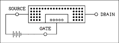
Figure 4.16 JFET with Reverse Bias on the Gate.
For a verbal description click here.
Figure 4.17 JFET Showing Pinch-off Effect.
For a verbal description click here.
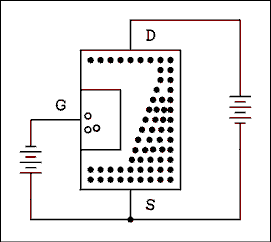
When a battery is connected across the ends of the channel, another effect becomes evident. Because the gate reduces the channel cross-section area, the resistance in the region of the gate is increased and most of the voltage which is applied will be dropped across the region occupied by the gate. This voltage drop causes the channel near the top of the gate (Figure 4.17) to be more positive than the channel near the bottom of the gate. The net voltage across the gate-channel junction is greater at the top than it is at the bottom. Hence, the depletion region will be wider at the top of the gate than it is at the bottom, as shown in Figure 4.17. As the voltage applied to the ends of the channel is increased, this effect is increased until the channel becomes a constant current device. The channel does not become a negative resistance device (current decreases as voltage increases). The voltage at which the channel changes from a resistive device to a constant current device is called the pinch-off voltage.
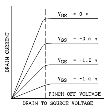
Figure 4.18 Drain Characteristics of a typical FET.
For a verbal description click here.
Figure 4.18 shows the drain characteristics of a typical junction field effect transistor. The semiconductor curve tracer in the laboratory will produce these curves on the screen of an oscilloscope. At drain-to-source voltages below the pinch-off voltage the drain-to-source path is a variable resistance while above the pinch-off voltage the drain-to- source path is a variable current source. Typical values for the pinch-off voltage are less than one volt.The Metal Oxide Semiconductor Field Effect Transistor.
The metal oxide semiconductor field effect transistor (MOSFET) is at the heart of most pocket calculators and microcomputers. Its construction is quite similar to the JFET except that the gate is a metal plate which is insulated from the channel by a thin layer of silicon dioxide instead of a region of opposite type semiconductor.The P-N junction in a JFET is not used as a diode. It operates in the reversed biased condition all of the time. The gate portion of the FET (P type semiconductor in the example shown) is only being used as a conductor. The depletion region on the gate side of the junction is being used as an insulator. Silicon dioxide is a much better insulator than is a reverse-biased P-N junction and metal is a better conductor than is P type semiconductor. So the replacements are made and the device works almost the same as it did before. In an N channel MOSFET if the gate is made negative with respect to the source the negative charge on the gate will repel negative charges in the semiconductor channel and create a depletion region around the gate the same as with a JFET. The principle of pinch-off works the same way as well.
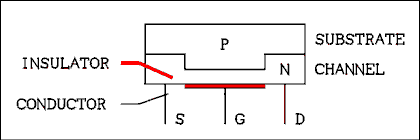
Figure 4.19 Metal Oxide Semiconductor FET.
For a verbal description click here.
The major difference between a JFET and a MOSFET is the gate or input resistance. For a JFET the typical input resistance is typically 1012 ohms while for a MOSFET the input resistance is typically 1016 ohms. MOSFETs are used in equipment which can measure currents in the picoampere range and below. Because of the high resistance of MOSFETs in a switching application, when they are off, they are really off. For this reason they find applications in very low power devices such as watches, calculators and lap-top computers.The substrate is the foundation on which the MOSFETs are constructed. In the case of discrete MOSFETs (as opposed to integrated circuits) the substrate may be brought out to a connecting lead of its own so the user may connect it as desired. The substrate is usually connected to the source although a P type substrate may be connected to the most negative point in a circuit. When MOSFETs appear in an integrated circuit, the substrate is the foundation on which the IC is constructed.
Enhancement Mode MOSFETs.
MOSFETs can be divided into two groups, depletion mode and enhancement mode. The group we have been talking about up until now are the depletion mode type, so called because they work by creating a depletion region in the channel. Depletion mode MOSFETs are "on" at zero gate voltage and a negative gate voltage will turn them "off".An enhancement mode MOSFET is "off" at zero gate voltage and a positive gate voltage (for an N channel) will turn it "on". The drawing of an enhancement mode MOSFET is shown in Figure 4.20.
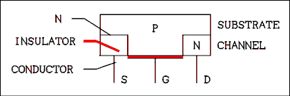
Figure 4.20 Enhancement Mode MOSFET.
For a verbal description click here.
In the case of an N channel MOSFET the substrate is P type semiconductor. Near the gate (between the source and drain) the substrate has been doped with both donor and acceptor impurities. The acceptors slightly outnumber the donors so the result is a lightly doped P type semiconductor. When the gate voltage is zero the P type semiconductor between the source and drain serves to block current between source and drain. When a positive voltage is placed on the gate, holes are repelled away from the gate. Once the holes are gone from this region, the donor impurities predominate and the material near the gate turns from P type to N type semiconductor. Current may now flow from source to drain.Enhancement mode MOSFETs are very rarely used as amplifiers. They most often appear in digital integrated circuits where they are used as switches.
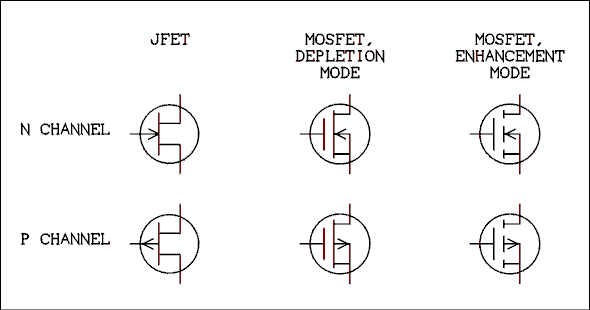
Figure 4.21 Schematic Symbols for Various Kinds of FETs.
For a verbal description click here.
Figure 4.21 shows schematic symbols for the various kinds of FETs. The FETs in the top row are N channel and the FETs in the bottom row are P channel. A good memory device is "the arrow always points toward the N type semiconductor". The bottom connection on each FET is the source. The connection on the left of each FET is the gate and the connection at the top is the drain. For MOSFETs the connection at center-right is the substrate. The substrate is shown connected internally to the source in these symbols. In some discrete MOSFETs the substrate is brought to a separate lead.For N channel FETs the drain is made more positive than the source. JFETs and depletion mode MOSFETs are fully on at zero gate potential. For operation as an amplifier, the gate is made more negative than the source. Enhancement mode MOSFETs are off at zero gate potential. For operation as an amplifier the gate is made more positive than the source.
For P channel FETs the drain is made more negative than the source. JFETs and depletion mode MOSFETs are fully on at zero gate potential. For operation as an amplifier, the gate is made more positive than the source. Enhancement mode MOSFETs are off at zero gate potential. For operation as an amplifier the gate is made more negative than the source.
4.5 The FET as a Switch.
FETs are usually not used to turn lamps and relay coils on and off. They find two major applications, as logic switches and as analog (or signal) switches. We will cover the latter application first.The term analog switch may seem to be mutually contradictory. What is meant is to interrupt an analog signal to turn it off and on as desired or to select among several sources of signal. An example of the latter is the source selector in a stereo receiver. The switch allows the user to select among several program sources. Classically this has been accomplished by a mechanical switch. Newer designs which include remote control require electronic switching. This electronic switching may be accomplished using an FET.
Figure 4.22 shows an FET being used to switch an analog signal. The control voltage is +15 volts to turn the switch on and -15 volts to turn the switch off. The signal applied to the input must never exceed approximately plus or minus 10 volts. If the input signal comes too close to +15 volts, the switch can be turned off when it is supposed to be on. If the input signal comes too close to -15 volts, the switch can be turned on when it is supposed to be off.
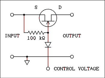
Figure 4.22 Analog Switch Using a JFET.
For a verbal description click here.
When the control voltage is positive, the diode is reverse biased, which disconnects the control voltage from the switched signal. The 100 k ohm resistor will cause the gate of the FET to be at the same potential as the source and the FET will be fully on. Signals applied to the input will appear at the output with little distortion or attenuation. When the control voltage is negative, the diode will be forward biased and the gate will be at approximately -15 volts. This will cause the FET to be turned off and very little or no signal from the input will be passed to the output. The 100 k ohm resistor will be connected from the -15 volt control signal to the signal source. In order for this circuit to work properly the signal source must have a low resistance for DC.Another type of analog switch is the CMOS (complementary MOS) device which comes in an integrated circuit. The IC operates from a single power supply (VDD) of up to 15 volts. The signal source must never go negative nor more positive than VDD. It is best for the AC signal source to be added to a DC of 1/2 VDD. If the signal part of the switch is forced outside of these limits by more than 0.7 volts the IC will, not may, but will be destroyed. The control voltage for this IC is zero to turn the switch off and VDD to turn the switch on.
A partial schematic diagram of the internal workings of this IC switch is shown in Figure 4.23. The triangle with a circle on its nose is an inverter. This is a switching device. If its input is zero, its output is VDD. If its input is VDD, its output is zero.
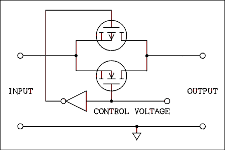
Figure 4.23 MOSFET Analog Switch.
For a verbal description click here.
The circuit is called complementary because it employs an N channel and a P channel MOSFET. When the control voltage is zero, the N channel FET has a gate voltage of zero and the P channel FET has a gate voltage of VDD. That turns both of them off. If the signal source is at a potential of VDD the P channel FET will still be off and the N channel FET will be negatively biased, which makes doubly certain that it will be off. If the signal source is at zero potential the N channel FET will still be off and the P channel FET will be positively biased, which makes doubly certain that it will be off. When the control input changes to VDD the N channel FET has a positive VDD on its gate while the P channel FET has zero potential on its gate. If the signal is at zero potential the N channel FET will be on but the P channel FET will be off. If the signal is at VDD the P channel FET will be on, but the N channel FET will be off. The two FETs are in parallel. So as long as one of them is on, the switch is on.The inverter is another example of how FETs are used as switches. Figure 4.24 shows the circuit of the inverter which was shown as a triangle in the circuit of Figure 4.23. When the input signal is at zero volts Q1 is biased fully on and Q2 is fully off. Thus the output is held to VDD. The output is high for a low input. If the input is VDD (high) Q1 is biased off (zero potential between gate and source) and Q2 is on. The output is low because it is held to ground by Q2. Whatever the state of the input, the output assumes the opposite state.

Figure 4.24 CMOS Inverter.
For a verbal description click here.
There are ICs which are known as invertors which contain six such circuits. Although they are not intended for use as analog devices, the input may be biased at 1/2 VDD and as such they make excellent amplifiers. (Which goes to show that if someone designs something, someone else will figure out a way to use it wrong and make it work.)Example 4.14.
A P channel depletion mode FET has -10 volts on its gate with respect to its source. Is it on or off?Solution:
A P channel depletion mode FET is on at zero potential and its drain current decreases as the gate is made positive. At +10 volts it would most likely be off but at -10 volts it is extremely on.Example 4.15.
An N channel enhancement mode MOSFET has a gate bias of zero volts. Is this FET on or off?Solution:
At zero volts between gate and source any enhancement mode MOSFET is off. The FET is off.4.6 The FET as an Amplifier.
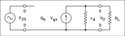
The FET has only two small-signal parameters, the drain resistance rd and the transfer conductance, called by contraction-loving electrical engineers transconductance Gm. The transconductance is defined as the AC drain current divided by the AC gate to source voltage with the drain to source voltage held constant.Gm = id / vgs with vds = 0 (4.37) The drain resistance is defined as the AC drain to source voltage divided by the AC drain current with the gate to source voltage held constant.
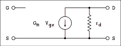
Figure 4.25 Small Signal Equivalent Circuit for an FET.
For a verbal description click here.
The Common Source Amplifier.
The common source equivalent circuit we will work from is shown in Figure 4.26. The input is an open circuit, as is the input of an FET. The output circuit consists of a current source which is dependent on the voltage between the gate and source. The drain resistance is in parallel with the current source. Any load is connected in parallel with the drain resistance.
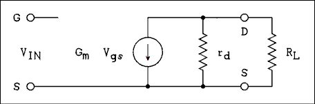
Figure 4.26 Equivalent Circuit of Common Source Amplifier.
For a verbal description click here.
The output voltage vo is the current source times the parallel combination of rd and RL.vo = -vin Gm rd RL / (rd + R/L) (4.19) Dividing through by vin and making the substitution AV = vo / vin we have,AV = -Gm rd RL / (rd + R/L) (4.20) where RL is the parallel combination of all resistors connected from the drain to AC ground.Amplifier Biasing.
A properly biased common source N channel JFET amplifier is shown in Figure 4.27. The battery VDD provides the positive bias for the drain and the battery VGG provides the negative bias for the gate. While this two-battery circuit will certainly work, it is not very practical.
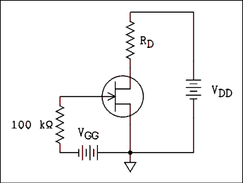
Figure 4.27 JFET Amplifier Using Battery Bias.
For a verbal description click here.
Figure 4.28a shows how the circuit may be rearranged without altering its operation. The negative connection point of VDD has been moved to the negative end of VGG, reducing VDD by the amount of VGG. This reduction is usually not significant enough to have any adverse effect. Notice that the polarity of VGG is the same as would be produced by the drain-source current flowing through a resistor in the source. Figure 4.28b shows the substitution of a resistor and a filter capacitor for the battery. The value of the source resistor sets the operating point.
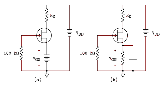
Figure 4.28 Converting Battery Biasing to Self Biasing.
For a verbal description click here.
Unlike for the BJT the operating point of the FET cannot be easily calculated. Some texts present a graphical solution which requires having a set of characteristic curves for the FET similar to those in Figure 4.18. Semiconductor manufacturers do not supply these curves for a very good reason. There is so much difference between FETs of the same type number that a set of curves would be useless. A semiconductor curve tracer interfaced to a computer and plotter could produce a set of curves for any individual FET and the graphic solution could be performed. Such a solution would be valid for only that one particular FET. Another FET would require another set of curves and a new graphical solution. We will not waste our time learning a useless procedure.The one and only advantage that FETs have over BJTs is their very high input resistance. In commercially designed equipment it is usual to see only one or two FETs among thirty or more BJTs. Even with such limited use, setting the operating point is a problem. There are two basic solutions. One is to use a trimming potentiometer (a screwdriver- adjusted variable resistor) as the source resistor as shown in Figure 4.29(a). Part of the calibration procedure includes setting the proper operating point of the FET amplifier. The other solution is to use the FET in conjunction with a BJT in an arrangement which will automatically set the operating point of the FET as shown in Figure 4.29(b).
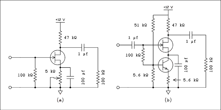
Figure 4.29 Practical JFET Amplifier.
For a verbal description click here.
Which one is used depends on who is to build the circuit. If the circuit is contained in a DIY article or a kit the reader or buyer is the one who constructs it. He does not receive a bill for his time at the end of each month so there is no cost associated with having him adjust the pot for the proper operating point.If the circuit is in a device which will be manufactured in the tens or hundreds of thousands and sold in retail stores the eventual owner cannot be held responsible for adjusting the pot. It must be done on the assembly line by a worker. It is an unavoidable fact that workers have to be paid. It is also a fact that workers do occasionally make errors. The expense of paying someone to adjust the pot will buy a lot of transistors. While the circuit at (b) is mor costly in terms of parts it is less expensive when fabrication costs are taken into account.
The (b) circuit works because the BJT sets the current through both transistors and holds it constant. The collector voltage, also the source voltage adjusts itself to what ever value is necessary to make the FET conduct the correct amount of current. The gate resistor is returned to the base to insure that the BJT will never be forced into saturation by the required gate to source voltage of the FET. The gate resistor in either circuit can easily go as high as 10 meg ohms if necessary.
Example 4.16.
In the circuit of Figure 4.29 the drain resistance of the FET is 130 k ohms and the transconductance is 600 micro mhos. What is the amplifier gain?Solution:
RL consists of the parallel combination of 47 k ohms and 100 k ohms, which is 32.0 k ohms. The gain of the amplifier isAV = -Gm rd RL / (rd + RL)
AV = -600 micro mhos x 130 k ohms x 32 k ohms / (130 k ohms + 32 k ohms) = -15.4
The Source-follower Amplifier.
Because the FET is used for its high input impedance, it is most often seen as a source-follower, as shown in Figure 4.30. The FET source-follower is characterized by very high input impedance, low output impedance and slightly less than unity gain.
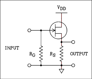
Figure 4.30 Source-follower Using N Channel JFET.
For a verbal descriptionclick here.
Figure 4.31 Equivalent Circuit of a Source-follower.
For a verbal description click here.
The equivalent circuit of a source-follower is shown in Figure 4.31. Summing the voltages around the outside loop we HaveVin = vgs + vo (4.21) In a source-follower the value of RL is usually much less than rd so we can neglect rd in the following equation. The output voltage is given byVo = vgs Gm RL (4.22) Solving equations 4.21 and 4.22 for vgs and setting them equal givesVin - vo = vo / (Gm RL) (4.23) Solving for vo / vin and remembering that AV is defined as vo / vin we have.AV = Gm RL / (Gm RL + 1) (4.24) As with the emitter-follower, the output impedance of the source-follower can be obtained by shorting the input, connecting a generator V across the output and determining the current I which flows. The output resistance is V/I. The equivalent circuit is shown in Figure 4.32.
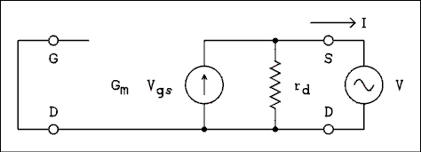
Figure 4.32 Finding Output Resistance of a Source-follower.
For a verbal description click here.
The current flowing through rd will be neglected. The current supplied by the generator is,I = Gm vgs (4.25) Because the input is short circuited vgs = V and so,RO = V / I = 1 / Gm. (4.26) The output resistance of a source-follower circuit is the parallel combination of the results of equation 4.26 and the resistor in the source of the FET. Note that unlike the emitter-follower the generator resistance has no effect on the output resistance.Example 4.17.
In the circuit of Figure 4.30 the value of RS is 1 k ohm and the transconductance of the FET is 3000 micro mhos. What are (a) the voltage gain and (b) the output resistance of the circuit?Solution:
(a) The gain is given byYou may be surprised by the low gain which is available from an FET source-follower. Designers seldom use a simple source-follower for just that reason. One very popular arrangement employs an N channel FET and a PNP BJT as shown in Figure 4.33. This circuit is often used as the input stage in oscilloscopes and AC voltmeters. This circuit is normally designed such that the collector current of the BJT is greater than the source current of the FET. This allows the BJT and the resistors to predominate in setting the operating point which eliminates the need for a trimming pot. Even so there is a DC offset between the input and output. The output may be anything from 1 to 4 volts more positive than the input. In DC coupled amplifiers such as those found in oscilloscopes this offset must be accounted for in some way to avoid adding it to the output.AV = Gm RL / (Gm RL + 1)
AV = 3000 micro mhos x 1 k ohm / (3000 micro mhos x 1 k ohm + 1) = 0.75
(b) The output resistance is
RO = 1 / Gm = 1 / (3000 micro mhos) = 333 ohms.
The output resistance is 333 ohms in parallel with 1 k ohm which is 250 ohms.
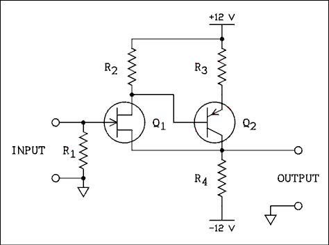
Figure 4.33 Unity Gain Impedance Buffer Using an FET.
For a verbal description click here.
This page last updated December 22, 2006.