![]()


![]()
![]()
![]()
![]()
![]()
![]()
![]()
![]()
|
Overview of Integrated Circuits An IC is an electronic network that has been fabricated on a single piece of semiconductor material such as silicon To accomplish this, the silicon surface is subjected to various processing steps in which dopants and other material layers are added with specific geometrical shapes. The IC therefore consists of a set of patterned layers of doped silicon, polysilicon, metal and insulating silicon dioxide.
Physical design of IC. The different material patterns may be stacked to produce either transistors for use in switching, or low resistance interconnects for transistor wiring. Physical Chip Design is the process whereby a circuit schematic of discrete components is transformed into a set of patterned layers in silicon
Layer patterning. The process used to transfer a pattern to a layer on the chip is called lithography.The lithographic sequence must be repeated for every layer which requires patterning.To design the patterns on each layer, a CAD layout editor is used o Layer distinguished by unique colour coding o Overlay of all patterned layers gives plan view of chip.
Example: CMOS inverter
Lithography & Pattern Transfer
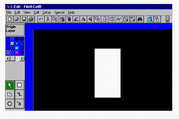
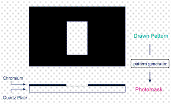
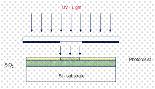
The major steps used in the lithography sequence are: o Drawing the patterns using a layout editor o Producing individual masks for each layer o Transferring the mask pattern to the wafer (printing) o Using processing techniques to physically pattern each layer Photolithography- pattern drawing
Photolithography – mask fabrication
Photolithography- printing
Photolithography- layer processing
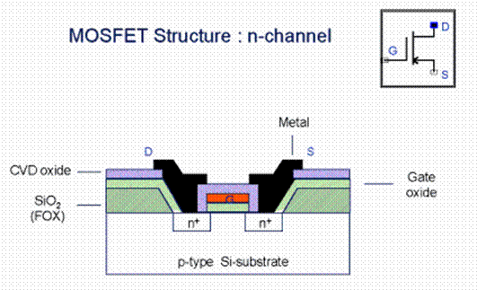
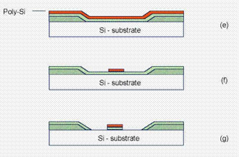
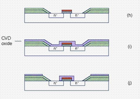
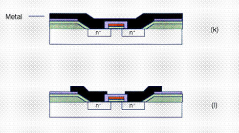
CMOS transistor fabrication: MOSFETs MOSFETs (metal oxide semiconductor field-effect transistor) are the transistors used in CMOS ICs. MOSFETs have become the primary switching devices in high-density (VLSI) IC design because they are extremely small, the ‘ drain’ and ‘source’ terminal are interchangeable and the device structures are very simple. MOSFET structure : n-channel
n-MOS devices: required material layers. º p-type substrate º thick field-oxide grown on substrate º n+ drain and source diffusion regions º high- quality thin gate oxide º polycrystalline silicon (poly-si) gate electrode º thick CVD oxide º aluminum interconnects to source and drain the fabrication of an n-MOS devices requires a photolithography stage to be performed on each of the above layers. Process flow for the fabrication of n-MOS devices
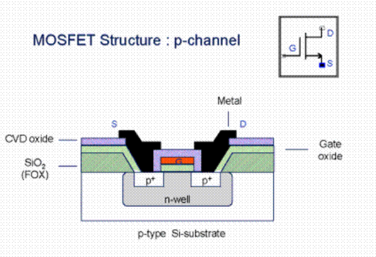
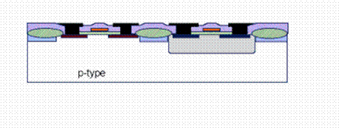
CMOS IC Fabrication: pMOS transistors A p-channel MOSFET has the same geometrical structure as an n-channel device but with reversed polarities o N-type » p-type o P-type » n-type To fabricate CMOS ICs it is necessary to construct both nMOS and pMOS transistors in a common substrate. For p-type substrates, localized n-type regions called “n-Wells” must be provided for use as the bulk of the pMOS transistors. MOSFET structure :p-channel
The CMOS fabrication sequence. There are 10 principal steps involved in CMOS fabrication: o N- Well formation (NWELL)
o Active area definition and isolation (ACTIVE)
o Gate oxide growth
o Poly-Si deposition and patterning (POLY1)
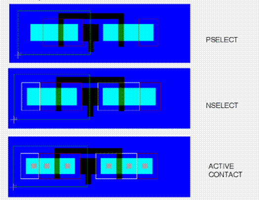
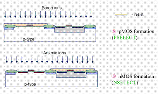
o pMOS formation (PSELECT) nMOS formation (NSELECT)
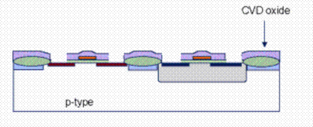
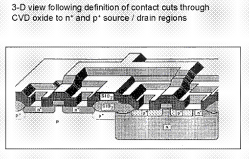
o Contact cuts to n+/p+ (CONTACT TO ACTIVE)
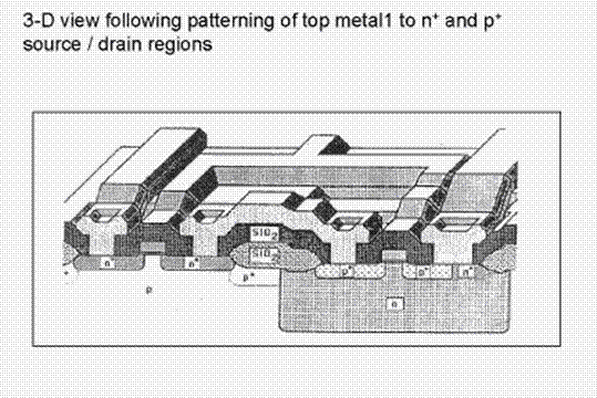
o Metal connections (METAL1)
o LTO oxide and Via definitions (VIA)
|