![]()


![]()
![]()
![]()
![]()
![]()
![]()
![]()
![]()
|
Characteristics of the CMOS Series
o Pin Compatibility 2 CMOS IC has pin compatibility when both of the pin configurations are the same. For example all pin 7 refers to GND. o Equivalent in function 2 CMOS IC has the same logic function. o Electrical Compatibility 2 IC are electrically compatible when it can be connected to each other directly.
o DC Supply Voltage CMOS devices are available in two different supply voltage categories, +5V and +3.3V o CMOS Logic Levels
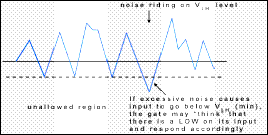
o Noise Immunity Noise is unwanted voltage that is induced in an electrical circuit and can present a threat to the proper operation of the circuit. In order not to be adversely affected by noise, a logic circuit must have a certain amount of noise immunity. This is the ability to tolerate a certain amount of unwanted voltage fluctuation on its inputs without changing its output state.
o Noise Margin A measure of a circuit’s noise immunity is called the noise margin. There are two values of noise margin specified for a given logic circuit: HIGH-level noise margin (VNH) and the LOW-level noise margin (VNL). These parameters are defines by the following equations: VNH = VOH (min) - VIH(min) VNL = VIL (max) - VOL(max)
(a) HIGH LEVEL noise margin
(b) LOW LEVEL noise margin
o Power Dissipation A logic gate draws current from the dc supply voltage source. When the gate is in HIGH output state, an amount of current designated by ICCH is drawn and in the LOW output state, a different amount of current, ICCL is drawn.
Power Dissipation (PD) = VCCICC ICC = ICCH + ICCL
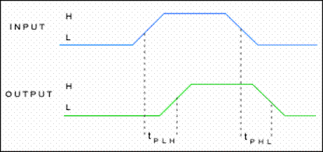
Power dissipation in CMOS is frequently dependent. It is extremely low under static (dc) conditions and increases as the frequency increases o Propagation Delay When a signal passes (propagates) through a logic circuit, it always experiences a time delay. A change in the output level always occur a short time, called the propagation delay time, later than the change in the input level that caused it. There are two types of propagation delay times specified for logic gates: tPHL: The time between a designated point on the input pulse and the corresponding point on the output pulse is changing from HIGH to LOW. tPLH: The time between a designated point on the input pulse and the corresponding point on the output pulse when the output is changing from LOW to HIGH.
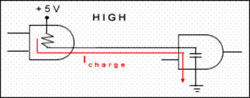
The propagation delay of a gate limits the frequency at which it can be operated. The greater the propagation delay, the lower the maximum frequency. Thus a higher-speed circuit is one that has a smaller propagation delay. o Speed-Power Product The speed-power product provides a basis for the comparison of logic circuits when both propagation delay and power dissipation are important considerations in the selection of the type of logic to be used in a certain application. The lower the speed-power product, the better. o Loading and Fan-Out When the output of a logic gate is connected to one or more inputs of other gates, a load on the driving gate is created. There is a limit to the number of load gate inputs that a given gate can drive. This limit is called the fan-out of the gate. CMOS Loading When the output of the driving gate is HIGH, the output capacitance of the load gate is charging through the output resistance of the driving gate. When the output of the driving gate is LOW, the capacitance is discharging.
When more load gates inputs are added to the driving gate output, the total capacitance increases because the input capacitance increases the charging and discharging times, thus reducing the maximum frequency at which rate can be operated. Therefore, the fan-out of a CMOS gate depends on the frequency of operation. The fewer the load gate inputs, the greater the maximum frequency.
|