![]()
![]()


![]()
![]()
![]()
![]()
![]()
![]()
![]()
![]()
|
Logic Circuit Types: CMOS Complementary Logic • CMOS Complementary Logic Circuits:– inverter– 2-input NAND– 2-NOR showing position of poly gates– complex logic gate [A(B+C)+(DE)]’ showing position of poly gates by ordering of device inputs• Each logic function is duplicated for both pull-down and pull-up logic tree– pull-down tree gives the zero entries of the truth table, i.e. implements the negative of the given function Z– pull-up tree is the dual of the pull-down tree, i.e. implements the true logic with each input negative-going• Advantages: low power, high noise margins, design ease, functionality• Disadvantage: high input capacitance reduces the ultimate performance
The AND/OR and Inverter Structure Creating "AND" and "OR" structures using MOSFET transistors is easily accomplished by placing the nmos and pmos transistors either in series (AND) or parallel (OR) as shown in Fig. 2 and 3. Shown in Fig. 2 (a) and (b) are two MOSFET transistors connected in series. The singular current path in both structures defines the "AND" operation. Shown in Fig. 3 (a) and (b) are two MOSFET transistors connected in parallel. The parallel current paths represent the "OR" structure.
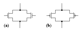
Fig. 2 (a) nmos "AND" structure (b) pmos "AND"
structure Fig. 3 (a) nmos "OR" structure (b) pmos "OR" structure
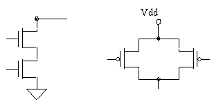
Figure 4 shows an nmos "AND" structure with the source
of M1 connected to ground (MOSFET Rule #2). An nmos switch is turned-on
when a logic high is applied to the gate input. The logic expression for
the circuit shown in Fig. 4 is
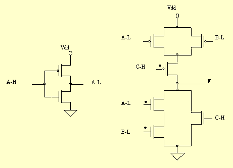
Fig. 4 An nmos Transistor Structure Realizing the expression F = (A B)-L Creating a CMOS inverter requires only one pmos and one nmos transistor. The nmos transistor provides the switch connection to ground when the input is a logic high while the pmos device provides the connection to the VDD power supply rail when the input to the inverter circuit is a logic low. This is consistent with MOSFET Rule #2. The transistor configuration for a CMOS inverter is shown in Fig. 5.
Fig. 5 The transistor view of a CMOS Inverter A Design Procedure for Creating CMOS Combinational Logic Circuits
The following design process [1] provides a method for obtaining an optimal CMOS combinational transistor structure given a functional (Boolean) expression. The method is based on the use of mixed logic concepts. The input variables should have a designated assertion level (i.e. Assert Low or Assert High). In CMOS designs, two transistor structures (one pmos and one nmos) are required for implementing the functional expression. In logic systems, the analogous expression defines what is required to generate the required output assertion level. The complementary expression, obtained by applying DeMorgan's theorem to the functional expression, defines the complementary structure. These two expressions, the analogous and the complementary, are then used to create the transistor network for a CMOS circuit. The design procedure is described as follows in five steps. 1. Identify the "most common" input level by examination of the input assertion levels. This requires that the input assertion levels be defined. An input variable containing a conflict is treated as if it has the opposite assertion level. The "most common" input level will be either "Low" or "High". This is determined by counting the number of asserted high or asserted low inputs after adjusting for conflicted inputs. 2. The "most common" input level is used to specify the type of transistors used for implementing the analogous structure
3. If there is not a "most common" input level then select the input level to be the opposite level of the required output assertion level. 4.(a) Create the analogous transistor structure directly from the functional logic expression. Use the transistor type specified in part 2 for creating the structure. 4.(b)The complementary structure is created by applying DeMorgan's theorem to the analogous expression. The transistor type is opposite to that used in part 4(a).
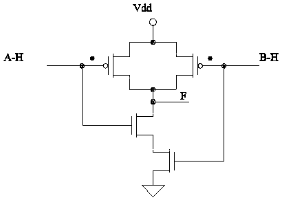
5. Assemble the analogous and complementary structures to create the full CMOS equivalent circuit. In some cases, an inverter must be added to the output of the circuit to correct the output assertion level. Example 1:
Given
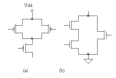
Fig. 6 The (a) analogous and (b) complementary
structures for Example 1
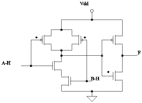
Fig. 7 The Complete Transistor Circuit for Realizing
the Expression Example 2:
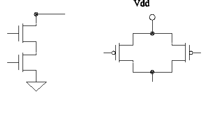
Given:
Fig. 8 The (a) analogous and (b) complementary structures for Example 2
Fig. 9 The Complete Transistor Circuit for Realizing
the Expression The procedures and results for creating the transistor equivalent circuits in Example 1 and Example 2 are the same except that the circuit in Example 2 required the placement of an inverter on the output to correct the assertion level to match desaign specifications. The logic circuit created in Example 1 is commonly called a Positive Logic NAND gate. The logic circuit created in Example 2 is commonly called a Positive Logic AND gate. This procedure can be easily applied to create NOR, OR, XOR, XNOR gates
Example 3:
Given:
Fig. 10 (a) the Analogous and (b) Complementary Structure
Fig. 11 The Complete Transistor Circuit for Realizing
the Expression
|