
Figure 6.1 Constant Voltage Biasing.
For a verbal description click here.
Chapter 6 Faults in Transistor Circuits.
6.1 Common Emitter Amplifier.
6.2 The Emitter-follower's Fatal Flaw.
6.3 AC Coupled Amplifiers.
6.4 DC Coupled Amplifiers.
6.5 Radio Frequency Amplifiers.
6.6 Switching Circuits.
Chapter 6.
Faults in Transistor Circuits.
Discrete transistor circuits are found in almost every area of electronics. Transistor circuitry is to be found in consumer, industrial, automotive and military electronics. The importance of knowing how to troubleshoot transistor circuits cannot be over-emphasized. In this chapter we will examine the minimal circuits that are the building blocks of larger circuits.Back to Fun with Transistors.
Back to Fun with TUBES.
Back to Table of Contents.
Back to top.
6.1 Common Emitter Amplifiers.
One of the most common uses of transistors is to provide signal amplification. The most common amplifier configuration is the common emitter amplifier.In this and following chapters we will refer to voltages at particular points. Everyone knows that there is no such thing as a voltage at a point, only voltages between two points. When we speak of a voltage at a point, the other point is assumed to be ground. Imagine that one lead of our voltmeter is connected to the ground point of the circuit. When we speak of the voltage at a point we are connecting the other lead of our voltmeter to that point. Thus the voltage at a point is the voltage between that point and ground.
Figure 6.1 Constant Voltage Biasing.
For a verbal description click here.
Figure 6.1 is the circuit of the most popular method of biasing a common emitter amplifier. Typical voltages for this circuit would be VE (emitter to ground voltage) = 1.13 volts, VB (base to ground) = 1.73 volts, and VC (collector to ground) = 6.79 volts.Suppose now that we observe the following voltages: VE = 1.5 volts, VB = 1.8 volts and VC = 12 volts.
The fact that VC = VCC indicates no voltage drop across the collector resistor and therefore no collector current. A shorted collector resistor can be ruled out because resistors rarely short.
VE - VB < 0.6 v could indicate a base-emitter short in the transistor, or could it? A base-emitter short would effectively place RE in parallel with R2. The parallel combination is (1.2 k ohms x 6.8 k ohms)/(1.2 k ohms + 6.8 k ohms) = 1.02 k ohms and the voltage divider equation gives a voltage at the base of 12 v x 1.02 k ohms /(1.02 k ohms + 39 k ohms) = 0.31 v. Since the measured voltage is 1.8 volts, a base to emitter short can be ruled out.
A short in the transistor involving the collector would make the collector and base voltages to be the same. Thus we can rule out a shorted transistor.
Because the voltage at the base is normal we can also rule out any trouble in R1 or R2.
If the collector resistor were open, the transistor collector would try to draw current and pull the collector voltage down to very near the emitter voltage. Thus we rule out the collector resistor.
After you have ruled out all other possibilities the one which remains is the answer. The emitter resistor open is the only thing not ruled out. Let us check the logic to see if it makes sense.
If the emitter resistor opens there can be no emitter current. With no emitter current there is also no collector current. No collector current means that there is no voltage drop across the collector resistor. Thus VC = VCC.
As a further consequence of no emitter current, the base-emitter junction will not be forward biased, VBE = 0.6 volts, which means that VE is closer than normal to VB. Since there is no base current, the voltage at the base will be normal or may increase slightly. All clues are consistent. The emitter resistor is open.
Suppose that we observe VE = 0, VB = 0 and VC = 12 volts. In this circuit there is no failure mode of the transistor which can make the base voltage zero. If R1 opens, there can be no current through R2 and no bias for the transistor. The transistor will be in cutoff; VE will be zero and VC = VCC. The answer must be R1 open.
Suppose we observe VE = 2.3 volts, VB = 2.9 volts and VC = 2.4 volts. There are two possibilities here, either the transistor is shorted (everything to everything) or the transistor is being driven into saturation. We will examine each possibility in turn.
If the transistor were shorted, the circuit would become that of figure 6.2. This places R1 in parallel with RC which is (39 k ohms x 5.6 k ohms)/(39 k ohms + 5.6 k ohms) = 4.90 k ohms and also R2 in parallel with RE (1.2 k ohms x 6.8 k ohms)/(1.2 k ohms + 6.8 k ohms) = 1.02 k ohms. The two parallel combinations make up a voltage divider. When we calculate the voltage we find 12 v x 1.02 k ohms /(1.02 k ohms + 4.90 k ohms) = 2.07 volts. If everything were shorted we should measure 2.07 volts at base, emitter and collector.
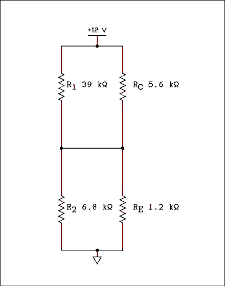
Figure 6.2 Figure 6.1 With a Shorted Transistor.
For a verbal description click here.
The only failure which could drive the transistor into saturation would be R2 open. If R2 opens, all of the current which flows through R1 will flow into the base of the transistor. We can calculate the base current as follows. From the voltage measurements above we see that the voltage at the base is approximately 3 volts. That leaves 9 volts to drop across R1. The current in R1 is 9 v / 39 k ohms = 230 microamps. If beta is 50 the collector current could be as high as 230 microamps x 50 = 11.5 mA. The resultant drop across RC is 11.5 mA x 5.6 k ohms = 64.4 volts. This is impossible! It is much greater than the power supply voltage. The transistor is in hard saturation. The fact that VB is different from VE is a strong (but not absolute) indication that the transistor is not shorted. It is time to shut down the power and make some ohmmeter tests.Ohmmeters and Transistors.
Ohmmeters must be used on transistor circuits with some caution, not because of any danger of damage to the circuit but because of the danger of arriving at the wrong conclusion. Analog and digital ohmmeters work quite differently and you can be badly misled if you fail to understand the difference.A digital ohmmeter applies a constant current source to the resistance under test and measures the voltage drop which results. Since the function V = I x R is linear, the scale is linear. The maximum voltage at full scale is 0.2 volts. This is not enough to forward bias a silicon P-N junction. What this means is that you cannot use a digital ohmmeter to test semiconductor devices. The meter will indicate over-range no matter what you do. You can use a digital ohmmeter to test resistors in transistor circuits without removing them from the circuit.
Many newer DMMs have a diode test position on the range switch. In this position the full-scale range is 2 volts (1.999) and a good P-N junction will indicate approximately 0.6 volts in the forward direction and over-range in the reverse direction.An analog ohmmeter applies a voltage to the resistance under test and measures the current which flows. The ohmmeter scale is very nonlinear because I = E / R is nonlinear. The voltage applied is 1.5 volts on all but the RX10,000 range, where it is 9 volts. This voltage is sufficient to forward bias P-N junctions. You can use an analog ohmmeter to test transistors out of circuit.In order to use an analog ohmmeter to test semiconductor devices you must know which lead of the ohmmeter is charged positively. In the case of the Simpson model 260 the terminal marked + is positive and the one marked "common" is negative. Many manufacturers are not as careful in designing their ohmmeter circuits. There are many analog ohmmeters on the market in which the terminal marked + is actually the negative side of the ohmmeter voltage source. The best way to find out is to use another test instrument to test the voltage at the ohmmeter terminals.
When you use an analog ohmmeter to test P-N junctions, you can determine if they are good, open or shorted.
When you connect the ohmmeter so as to forward bias the junction it will indicate a relatively low resistance. The actual value will be different on different ranges because a P-N junction does not obey Ohm's law.
When you connect the ohmmeter so as to reverse bias the junction the meter will indicate infinite resistance.
If a P-N junction is shorted the ohmmeter will show the same low resistance value in both directions. This value may range from 0 to a few ohms and will likely obey Ohm's law.
If the P-N junction is open it will indicate infinite resistance in both directions.
Example 6.1.
In the circuit of figure 6.3 the normal voltages are VE = 1.1 v, VB = 1.8 v and VC = 10.9 v. After the circuit develops a fault a low cost analog VOM is used to make the following voltage measurements: VE, VB and VC are all approximately 6 volts. What is wrong?

Figure 6.3 Circuit for Example 6.1.
For a verbal description click here.
Solution:
With all voltages being the same, our first conclusion might be that the transistor is totally shorted. If the transistor were shorted (everything to everything) the circuit of figure 6.4 would result. This fault places R1 in parallel with RC and R2 in parallel with RE. The two parallel combinations form a voltage divider across the power supply.

Figure 6.4 Figure 6.3 With a Shorted Transistor.
For a verbal description click here.
R1 in parallel with RC is (27 k ohms x 4.7 k ohms) / (27 k ohms + 4.7 k ohms) = 4.0 k ohms. R2 in parallel with RE is (4.7 k ohms x 4.7 k ohms) / (4.7 k ohms + 4.7 k ohms) = 2.35 k ohms. Applying the voltage divider equation gives VEBC = 12 v x 2.35 k ohms / (2.35 k ohms + 4.0 k ohms) = 4.44 volts. This seems rather far away from the measured value of 6 volts.If R2 opened the circuit would become that of figure 6.5.

Figure 6.5 Figure 6.3 With R2 Open.
For a verbal description click here.
This would cause the transistor to be driven into hard saturation. The measured voltage indicates a drop of approximately 6 volts across R1. Since all of the current through R1 flows into the base of the transistor, the base current is 6 v / 27 k ohms = 220 microamps. Assuming 50 as a reasonable value for beta, the collector current could be as high as 50 x 220 microamps = 11 mA. If this current could flow through RC it would produce a voltage drop of 11 mA x 4.7 k ohms = 51.7 volts. This impossible voltage indicates that the transistor is in hard saturation. A transistor which is held in saturation has the equivalent circuit of figure 6.6.

Figure 6.6 Equivalent Circuit of Figure 6.3 With R2 Open.
For a verbal description click here.
If we neglect the drop across the diode in figure 6.6, we have a voltage divider consisting of R1 in parallel with RC and the parallel combination is in series with RE. The voltage at all elements is VEBC = 12 v x 4.7 k ohms / (4.7 k ohms + 4.0 k ohms) = 6.48 volts.The possibility that the transistor is shorted gives a voltage of 4.44 volts and the possibility that R2 is open gives 6.48 volts. The original measurement was approximately 6 volts. 6.48 is closer to 6 than 4.44 v; therefore, the answer must be that R2 is open. If the transistor is good, the voltage at the base would be 0.6 or 0.7 volts higher than that at the emitter. Since our cheap voltmeter did not show us this difference between 6 and 6.6 volts, it could not show us the difference between 6 and 6.48 volts.
Troubleshooting Without a Voltage Chart.
While the major manufacturers are very good about providing typical AC and DC voltage measurements, these companies can be counted on the fingers of one hand. There are dozens of medium sized and hundreds of small manufacturers who provide electronic equipment to industry and education. The owner's manuals provided by these lesser companies range from rough to downright primitive. A schematic diagram is about all you can expect. If you get a circuit board layout, consider yourself indeed fortunate. If you do get normal operating voltages, buy stock in the company while it is still cheap.Small companies are often able to provide quality equipment at a lower price than a large company would ask. It is for this reason that you are likely to encounter such equipment in your career.
Suppose you are working on a piece of equipment from one of these smaller manufacturers and you measure the collector voltage of a transistor. You don't know any more after you make the measurement than you did before you made it. The reason is, of course, you don't know what the voltage is supposed to be.
If you are not given the voltages, you must calculate them yourself. Let us calculate the voltages in figure 6.1.
Note: If you follow the links below, use your back button to return here.First, we will calculate the Thevenin equivalent of R1 and R2 in the base circuit from Equations 4.18 and 4.19. VBB = 12 v x 6.8 k ohms / (6.8 k ohms + 39 k ohms) = 1.78 volts. RB = 6.8 k ohms x 39 k ohms / (6.8 k ohms + 39 k ohms) = 5.79 k ohms.If we don't know beta we can apply Equation 4.24.
Ic = (VBB - VBE)/RE = (1.78 v - 0.6 v)/1.2 k ohms = 0.983 mA. We may want to use Equation 4.23. To do so we must make a guess as to the beta of the transistor. It will do little good to look up the transistor in a transistor manual. Values of beta even for transistors of the same type number can range from 25 to 250 and are listed as such in the manual.Let us make a slightly pessimistic guess that the transistor's beta is 50.
Ic = (VBB - VBE)/(RE + RB/beta) To calculate VE we must know IE. IE = IC (1 + Beta) / BetaIc = (1.78 v - 0.6 v)/(1.2 k ohms + 5.79 k ohms / 50) = 0.897 mA.
IE =0.897 (51/50) = 0.915 mA. VE = IE RE = 0.915 x 1200 = 1.098 Volts.The voltage at the collector is equal to VCC - IC x RC. VC = 12 v - 0.897 mA x 5.6 k ohms = 6.98 volts.
Example 6.2.
In figure 6.3 change R1 to 270 k ohms and R2 to 82 k ohms. Calculate the values of VB, VE and VC.Solution:
Let us calculate the Thevenin values for the voltage divider circuit of R1 and R2. VBB = 12 v x 82 k ohms / (270 k ohms + 82 k ohms) = 2.80 v. RB = 82 k ohms x 270 k ohms / (82 k ohms + 270 k ohms) = 62.9 k ohms.By now you may be wondering if all of these calculations are worth the effort. You are likely thinking that you could change a resistor or transistor while someone else is making all of those calculations. Giving all of the details of a calculation in printed or written form always takes longer than it would on a calculator. An experienced person can finish the above calculations, using a pocket calculator, before the soldering iron gets hot.Equation 4.24 depends on the voltage drop across RB being small. Because of the large value of RB in this problem we cannot ignore this voltage drop. We must use Equation 4.23.
IC = (VBB - VBE)/(RE + RB/beta) VE = RE IC (Beta + 1) / BetaIC = (2.80 v - 0.6 v)/(1.2 k ohms + 62.9 k ohms/50) = .895 mA.
VE = 1200 0.895 (51/50) = 1.095 volts.
The voltage at the base is VB = VE + 0.6 = 1.695 volts.
The voltage at the collector is equal to VCC - IC x RC. VC = 12 v - 0.895 mA x 5.6 k ohms = 6.99 volts.
Another way is to have a computer program that will perform the calculations and show the results. Such a program may be downloaded from this location. This program only works on windows computers in north America. Clicking on the link above will initiate download.
You will find that the program gives slightly different results from the calculations performed above. The computer program uses the exact equation which was derived in chapter 4 section 3 of Electronics for Physicists. Equation 4.22 is the most accurate and that was used in the program since there is no point in using approximations in a program. Most of the above results were obtained with equation 4.23 which neglects a Beta / (Beta + 1) term.
- After clicking the link you will be asked if you want to open or save the file. Select save.
- You can save it anywhere you want but remember where you saved it. I have a folder in My Documents named AAA as a place to put such files.
- After download completes close the dialog box if you didn't check the box that says "Close this dialog box when download completes.
- Open windows explorer and navigate to the folder where you downloaded the file. Select "Transistor_Q_Point.zip" in the left hand window and it will be unzipped and the three files it contains will display in the right hand window.
- If "Transistor_Q_Point.zip" won't show in the left hand window, double click it in the right hand window. A new explorer window will open and three files will be displayed in it.
- Double click "setup.exe" and the program will begin to install.
- Accept all defaults unless you have a strong reason for doing otherwise.
- When the installation is finished you will see the message "Transistor Q Point was successfully installed."
If your computer is not close to your workbench you may be very tempted by the process of "shotgunning" described in chapter 4 but beware. You can afford to fire the shotgun only once. If you fire it and miss, you could be in trouble with your supervisor or customer. There are faults which can be misleading as to which stage the trouble is in.
There are other faults which can occur in a common emitter circuit. These faults will be covered in sections 6.3 and 6.4.
Back to Fun with Transistors.
Back to Fun with TUBES.
Back to Table of Contents.
Back to top.
6.2 The Emitter-Follower's Fatal Flaw.
The fatal flaw in the emitter-follower is that the transistor can fail and the circuit can continue to function under some circumstances. A "tape output" on a stereo receiver might drive one tape deck but not another; a regulated power supply which is rated to deliver 500 mA will begin to current limit at 25 mA; an oscilloscope which, when new, had a bandwidth of 100 MHz, now has only a 30 MHz bandwidth. Faults involving the emitter-follower can be so subtle that they can go undiscovered for months or even years.When an NPN transistor develops a base-emitter short it becomes equivalent to the circuit of figure 6.7.

Figure 6.7 NPN Transistor with B to E Short.
For a verbal description click here.

Figure 6.8 Emitter-Follower Circuit.
For a verbal description click here.
If we put this shorted transistor into the emitter-follower circuit of figure 6.8 the result is the circuit of figure 6.9.

Figure 6.9 Emitter-Follower with Shorted NPN BJT.
For a verbal description click here.
The diode which was the base-collector junction in the former transistor is now just a diode. In the circuit of figure 6.9 it will always be reversed biased. We may leave out this reversed-biased diode and our former emitter-follower circuit now is that of figure 6.10.

Figure 6.10 Equivalent Circuit of Emitter-Follower with Shorted BJT.
For a verbal description click here.
An emitter-follower has a voltage gain of approximately unity. The circuit of figure 6.10 has a voltage gain of unity, which is one of the reasons why the fault can be so hard to find. An emitter-follower has a current gain of approximately the beta of the transistor. The circuit of figure 6.10 has a current gain of less than unity, which is the reason it needs to be repaired.Tape Output Buffer Amplifier.
Consider the AC coupled emitter-follower of figure 6.11. This circuit is often incorporated in the "tape output" circuit of stereo receivers or in the output circuit of tape decks or CD players. Although most tape decks have a high input impedance, occasionally one will come along which has a medium or even low input impedance. I happen to own one that has a 10 k ohm input resistance. If a consumer has more than one tape deck it is likely that "Y" connectors will be used to parallel the inputs of the decks on the one tape output. This is why the designer of the receiver put an emitter-follower in the tape output circuit.

Figure 6.11 AC Coupled Emitter-Follower Circuit.
For a verbal description click here.
If the transistor in figure 6.11 develops a base-emitter short, the circuit will become that of figure 6.12. If the receiver is being used with one tape deck which has a high input impedance the fault may never be noticed. The fault may show up when the consumer tries to add another tape deck to the system.

Figure 6.12 Emitter-follower with Base to Emitter Short.
For a verbal description click here.
The consumer will first blame the new tape deck. After being assured by the service technician that there is nothing wrong with the new deck, the receiver is likely to be the next item to appear on the service bench. The technician is unlikely to place any load on the tape outputs and the fault will not be found. The end result is an angry consumer who may never do business with that technician again.A fault in an emitter-follower can be more easily found by DC analysis than by AC analysis. A typical set of DC voltages for the circuit of figure 6.11 is, VE = 7.3 volts and VB = 8.0 volts. Because the collector is connected directly to the +12 volt line the collector voltage will always be 12 volts. If the transistor develops a base to emitter short, R2 will be placed in parallel with RE and the equivalent resistance is (4.7 k ohms x 22 k ohms) / (4.7 k ohms + 22 k ohms) = 3.87 k ohms. The voltage divider now consists of a 10 k ohms and a 3.87 k ohms resistor. The voltage at base and emitter is 12 v x 3.87 k ohms / (3.87 k ohms + 10 k ohms) = 3.35 volts.
If measurement of DC voltages, (static testing), in an emitter-follower reveals voltages much lower than normal, you can bet your VOM that there is trouble in the circuit.
Wide Band Amplifier.
Now consider the circuit of figure 6.13. This circuit is typical of circuits found in the vertical amplifiers of oscilloscopes. These amplifiers are always differential or push-pull in configuration. The other half of the amplifier would be exactly like the half which is shown.The emitter bypass capacitors have not been omitted from the drawing; there are none in the circuit. This introduces a large amount of emitter degeneration or negative feedback. Like all negative feedback this emitter degeneration increases the upper limit of frequency response. The designers are giving up gain to get increased bandwidth. The gain of the common emitter stages is approximately RC/RE.

Figure 6.13 Wide Band Amplifier.
For a verbal description click here.
The emitter-follower Q2 would seem to be completely superfluous. The output impedance of the Q1 common emitter stage is the same as the collector resistor, 1 k ohms. The input impedance of the Q3 common emitter stage is approximately equal to RE x beta, or about 17 k ohms. A 1 k ohms source certainly does not need any help to drive a 17 k ohms load. If resistance was all there was to it then Q2 would be superfluous.Two factors which control the upper frequency limit of an amplifier are the characteristics of the transistors and the capacitance in the circuit. Assuming that Q1, Q2 and Q3 are the best that money can buy, the upper frequency limit of the Q1 stage will be determined by the total amount of capacitance from the collector of Q1 to ground. This capacitance is the output capacitance of Q1 and its printed circuitry, plus the input capacitance of the following stage.
If the following stage were a common emitter, this input capacitance would be made up of the input capacitance of the transistor plus the capacitance of the printed circuitry plus the Miller capacitance of the common emitter stage. If the stage following Q1 is an emitter-follower, there is no Miller capacitance. The purpose of the emitter-follower stage (Q2) is to isolate the Miller capacitance of Q3 from the output of Q1.
If Q2 develops a base-emitter short, the Miller capacitance of Q3 is no longer isolated from the output of Q1 and the frequency response of the amplifier will be impaired.
DC measurements may not reveal the fault because the emitter-follower is not doing any work at DC. The fault may show up if careful measurement is made of the base to emitter voltage of Q2 using a DMM. But even this measurement is not an ironclad guarantee of finding the trouble. It usually comes down to pulling the transistors from the board and testing them out of circuit.
If a scope with impaired frequency response comes to the bench of a technician who is unaware of this kind of fault, he or she may work for days and not find the cause. It may even get as far as recommending that the scope be junked.
Example 6.3.
In the circuit of figure 6.13 the output capacitance of the Q1 stage is 1 picofarad and the input capacitance of the Q2 stage is also 1 pf. The input capacitance of Q3 is 1 pf and the Miller capacitance is 4 pf. What are (a) the normal upper frequency limit of the amplifier and (b) the upper frequency limit if Q2 develops a base to emitter short?Solution:
(a) When the circuit is operating normally the capacitance across R1 is 1 pf + 1 pf = 2 picofarads. fC = 1 / (2 x � x R x C) = 1 / (6.28 x 1 k ohms x 2 pf) = 79.6 Mhz. (b) Even if Q2 is shorted its capacitance does not disappear. The total capacitance is now CT = CoQ1 + CiQ2 + CiQ3 + CmQ3 CT = 1 pf + 1 pf + 1 pf + 4 pf = 7 pf. The new corner frequency is fC = 1 / (6.28 x 7 pf x 1 k ohms) = 22.7 Mhz.Regulated power supply.
You may not have realized it but the pass transistor in a regulated power supply is an emitter follower. The circuit of a simple adjustable voltage power supply is shown in figure 6.14. The diagram has been arranged in such a way as to emphasize the fact that the pass transistor is an emitter- follower.
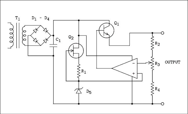
Figure 6.14 Regulated Power Supply.
For a verbal description click here.
Suppose that Q1 develops a base to emitter short. The circuit reduces to that of figure 6.15. This is just a noninverting amplifier whose gain is set by R1, R2, and R3. It is amplifying the voltage of the zener diode. That is all any regulated power supply does no matter how complex it may appear.

Figure 6.15 Regulated Power Supply After Q1 Develops a Base-Emitter Short.
For a verbal description click here.
If a power supply with a shorted pass transistor comes to your service bench you may wonder at first if it was operator trouble rather than equipment trouble. The output voltage comes up, it can be adjusted over its full range (assuming that the unit you are working on is adjustable) and the scope does not show any ripple. If you send it back to the lab with no further tests, it will be back on your bench within a day.The output of a typical op amp (operational amplifier) will deliver about 25 mA. This is sufficient to supply current to the voltage adjust resistors and the power supply will function normally as long as there is no large load on the output.
When a power supply comes to your service bench you should always test the supply at its specified maximum current.

Figure 6.16 Simple Regulated Power Supply.
For a verbal description click here.
Many regulated power supplies use a Darlington connected pair as the pass transistor, figure 6.16. If Q2 develops a base to emitter short the power supply will still work and will likely deliver an appreciable current, several hundred milliamperes. However, it will not perform up to its specified maximum current.If Q1 develops a base to emitter short, Q2 will try to take over the duties of Q1. Q2 is not equipped with a large heat sink and will overheat very quickly. The power supply will seem to work normally for a short time and then catastrophically fail. Q2 will likely short everything to everything. The output voltage will go above specified maximum and stay there.
If both transistors in a Darlington pair have base to emitter shorts, the supply will be down to the bare op amp as shown in Figure 6.15. If you replace only one of the defective transistors you will create one of the situations described above.
The Cause of the Short.
You may be wondering how a base-emitter short can happen. The usual cause of any failure is difficult to pinpoint. Part of the fatal flaw in the emitter-follower is that it has its cause of failure built in.Consider the circuit of figure 6.11 again. If there is no load connected to the output when the power is turned on, C2 will remain discharged. If the output is then shorted momentarily to ground, the capacitor will be charged through the emitter of the transistor. The pulse of current is short, but it can be several amperes in magnitude. This extremely large current pulse can burn out the base-emitter junction of a small transistor. The collector-base junction is larger in cross-section area and is usually not damaged.
It is possible to burn out the tape output buffer in a stereo receiver very easily. If the owner makes connections to the tape output with power turned on, the capacitor in the output will start out with no charge on it. In the process of connecting the cables it is possible to momentarily short the output and there goes the emitter-follower transistor. This is a documented and repeatable failure in a stereo receiver from a well known manufacturer.
A modification which will prevent burning out the transistor is to connect a resistor of about 470 k ohms from ground to the terminal marked "output" in figure 6.11. This will make sure that C2 gets charged even if there is nothing connected to the output. It is the charging of C2 through a dead short, not a resistor, which can destroy the transistor.
In the case of a power supply the pass transistors can be zapped if the power supply is forced to charge a large external capacitor each time the power supply is turned on. The current limiting circuits should prevent such damage but if it is a little slow to respond the pass transistors may experience a large amplitude current pulse.
We have cited only three uses of emitter-followers, there are many others. All are subject to the same kind of failure and all can be a little tricky to find.
Back to Fun with Transistors.
Back to Fun with TUBES.
Back to Table of Contents.
Back to top.
6.3 AC Coupled Amplifiers.
AC coupled amplifiers make up a significant percentage of amplifier circuits. They are used in audio, radio frequency and industrial applications.An AC coupled amplifier is shown in figure 6.17. The emitter resistors are bypassed to increase the gain to the maximum. Capacitor C1 prevents whatever may be connected to the input from upsetting the base bias of Q1. C3 prevents the DC voltage at the collector of Q1 from upsetting the base bias of Q2 and C5 prevents the DC voltage at the collector of Q2 from reaching whatever is connected to the output.
DC Voltage Measurements.
If an emitter bypass capacitor shorts, the emitter voltage of that transistor will be zero. The voltage divider in the base will cause a very large base current to flow, which will drive the transistor into hard saturation. The typical voltages for a shorted bypass capacitor will be VE = 0 v, VB = 0.7 v and VC = 0.1 v.

Figure 6.17 Two Stage Common Emitter Amplifier.
For a verbal description click here.
The results of a short in C1 are difficult to predict without knowing what is connected to the input. Suppose that a dynamic microphone is connected there. It is typical for a dynamic microphone to have a DC resistance of only a few tens of ohms. If C1 shorts, it will remove all bias from the base of Q1 and cause Q1 to be driven into cutoff. Typical voltages for this condition will be VE = 0 v, VB = 0 v and VC = VCC.If C3 shorts, the result will depend on whether the voltage at the collector of Q1 is greater than or less than the voltage at the base of Q2. The two voltages will become equal and Q2 will be in either saturation or cutoff depending on whether VCQ1 is greater or less than VBQ2. Typical voltages cannot be given because they depend on the values of the resistors.
The effect of a short in C5 depends on what is connected to the output. If it were one side of a pair of headphones, the DC resistance would be very low, about 6 ohms. This would pull the collector voltage down and forward bias the base-collector junction. The transistor may not be damaged but it certainly will not amplify. Typical voltages would likely be VE = 0 v, VB = 0.7 v and VC = 0 volts.
AC Voltage Measurements.
If you are signal tracing instead of making static tests, you will see the signal suddenly disappear at the defect. A transistor which is in cutoff or saturation does not provide a signal path. Some types of faults can make you think that the trouble is in the stage ahead of where it actually is.Suppose that Q2 in figure 6.17 develops a base-emitter short. The emitter is connected to ground through a capacitor. Because the base is shorted to the emitter, the base will be at AC ground potential. C3 also has a low reactance for AC and so the collector of Q1 is effectively shorted to ground for AC. The signal is no longer present at the collector of Q1 because it is shorted out by the series combination of C3, the base to emitter short in Q2 and C4.
When signal tracing, you would find signal at the base of Q1 and no signal at the collector of Q1. Your first conclusion would be that the trouble is in the Q1 stage. DC measurements would reveal that all in the Q1 stage is well. DC measurements in the Q2 stage will reveal the base to emitter short. This false clue is a very common phenomenon in transistor circuits.
A transistor which is being driven into hard saturation may appear as a short circuit to the signal. When the AC signal disappears, you must check the stage just after the point where the signal disappeared as well as the one where it disappeared.
Back to Fun with Transistors.
Back to Fun with TUBES.
Back to Table of Contents.
Back to top.
6.4 DC Coupled Amplifiers.
A DC coupled amplifier is one in which the stages are coupled together without using capacitors. Sometimes this is done because the amplifier must have gain all the way down to and including DC. Sometimes the reason is economics.One of the miniature capacitors which are used in transistor circuits can cost 4 or 5 times as much as a resistor. The capacitors may even cost more than the transistors. Therefore, if it is possible to replace one capacitor with three resistors, the design engineer will do it. Even in circuits where the signals are AC only, it is very common to see groups of two, three or even four stages which are DC coupled.
A two-transistor DC coupled gain block is shown in figure 6.18. R4 is present to allow negative feedback to be applied to the emitter of Q1. If no feedback is to be connected, R4 can be replaced with a piece of wire. With R4 = 0, this circuit can provide the same amount of gain as the circuit of figure 6.17. The circuit of figure 6.18 with R4 = 0 does the same job with only 5 resistors and 3 capacitors, as opposed to 8 resistors and 5 capacitors for figure 6.17.

Figure 6.18, Two-stage DC Coupled Amplifier.
For a verbal description click here.
Operating point stabilization (DC feedback) is provided by R1 and R2 from the emitter of Q2 to the base of Q1. AC feedback along this path is prevented by C2, which bypasses AC signals at the emitter of Q2 to ground.AC feedback is often added to this circuit by making R4 some low value, say 100 ohms, and coupling signal from the output back to the emitter of Q1.
If Q1 goes totally shorted, all of the voltages in the circuit will go nearly to zero except the collector of Q2, which will go up to VCC. The reason for this is as follows. When Q1 shorts out, all of its voltages will be equal to each other. R4, if it exists at all, is a low value and its voltage drop is very small. The short in Q1 will pull the base of Q2 down and send Q2 into cutoff.
If Q2 goes totally shorted, the emitter voltage of Q2 will remain normal, provided that R5 and R6 are not too low compared to R3. The DC feedback from the emitter of Q2 to the base of Q1 is responsible for this. The voltages at the collector and base of Q2 will be equal to the emitter voltage. The circuit with this defect will not provide gain for AC because C2 bypasses all signals to ground.
Example 6.4.
The normal voltage chart for the circuit of figure 6.18 is as follows.
VE VB VC Q1 0 v 0.6 v 4.0 v Q2 3.4 v 4.0 v 8.3 v A fault develops and the voltages become:
VE VB VC Q1 0 v 0.6 v 1.6 v Q2 1.0 v 1.6 v 10.9 v What is wrong?
Solution:
The transistors are not shorted because both have VB > VE and VC > VB. We conclude that both transistors are good. The voltage drop across R1 is 0.4 volts. This indicates that the current through R1 is not what it used to be. This could only be caused by R2 being open.In example 6.4, the feedback is what causes the circuit to behave in the way it does. The voltage at the emitter of Q2 will be adjusted to whatever is necessary to make the voltage at the base of Q1 be 0.6 volts. As long as R1 and R2 are intact the emitter of Q2 adjusts to 3.4 v to forward bias Q1 by just the right amount. In this circuit you might assume that if R2 opened, the transistor would be driven into hard saturation. But if the base is receiving too much bias the collector voltage of Q1 will come down and the emitter voltage of Q2 will follow. The emitter of Q2 will assume whatever voltage is necessary to provide just the right amount of bias to the base of Q1.
This is another one of those circuits which will continue to work even with a defect, especially if there is AC feedback to the emitter of Q1. The circuit will function quite normally for small signals. On larger signals the positive peaks will be clipped off. This is because the voltage at the collector of Q2 (10.9 volts) can only go up to 12 volts but it can go down to about 1 volt.
If R3 opens there will be no current path from the collector of Q1 to VCC. The collector of Q1 which is also the base of Q2 will fall to its lowest possible potential. The voltages will be much the same as if Q1 had shorted, except if R4 is present, there will be absolutely no voltage drop across it because there is no current through it.
If R5 opened, the voltage at the collector of Q1 would fall until it became equal to the emitter voltage. All other voltages in the circuit may be normal, depending on the relative values of R3 and R6, because of the DC feedback through R1 and R2.
When R5 opens, R3 and R6 become a voltage divider with the base-emitter junction of Q2 acting as a forward biased diode. If R3 is much larger than R6 it will be unable to pull the voltage up to the normal emitter voltage. If the voltage divider of R3 and R6 can assume a voltage greater than the normal emitter voltage of Q2, the collector current of Q1 will pull the voltage down to the normal value.
Depending on the load impedance the circuit may still provide gain while adding some distortion. However, the sign of the gain will be changed. When the circuit is working normally it is a noninverting amplifier. When R5 opens, Q2 is no longer an inverting amplifier. With only Q1 doing any amplifying, the overall gain of the circuit is inverting. If this circuit is in the middle of a larger feedback loop the feedback can change from negative to positive.
If R6 opens, the emitter current of Q2 will be only that which flows through R1 and R2. The voltage at the collector of Q2 will rise to very nearly VCC. All other voltages in the circuit will be normal because of the regulating effect of the feedback.
Figure 6.19 shows a configuration involving an NPN and a PNP transistor. This circuit is stabilized by DC feedback from the tap on the collector resistor of Q2 which feeds back a portion of the output voltage to the emitter of Q1. The voltage at the node between R4 and R5 will adjust itself until Q1 has just the right collector current to provide just the right amount of bias to Q2.

Figure 6.19 Complementary DC Coupled Amplifier.
For a verbal description click here.
The feedback path also passes AC. The gain of this circuit is set at 10. If higher gain is required, the variation of figure 6.20 may be used.If Q1 in figure 6.19 shorts, it will effectively place a 100 ohm resistor from the base of Q2 to ground. This will unquestionably drive Q2 into hard saturation. The base current will be approximately 120 mA, assuming a 12 volt power supply. This excessive base current may destroy Q2 as well. In the circuit of figure 6.20 R4 will prevent excessive current from flowing and Q2 will likely survive.
In figure 6.19 if R2 opens, Q1 will receive constant current bias through R1. This will increase the collector current of Q1 and in turn increase the collector current of Q2, driving it into saturation. The voltage at the collector of Q2 will be 12 volts but the voltage at the emitter of Q1 will be higher than the expected value of 1.2 volts. The reason is the emitter current of Q1 has become significant compared to the current flowing through R4 and R5. In a test circuit with R2 open the emitter voltage of Q1 was 3 volts.
If R3 opens, the effect may never be noticed. A slight reduction of bandwidth at high signal levels will be the only observable effect.
If R5 opens, the voltage at the collector of Q2 will fall to about 0.6 volts. This is because the feedback in the circuit will try to keep Q1 biased just right. The base of Q1 is set at 1.2 volts by R1 and R2. In order to keep Q1 properly biased, the emitter voltage must be 0.6 volts. With R5 open the voltage drop across R4 is extremely small. Thus the collector of Q2 will be at 0.6 volts.
If R4 opens, the result will be to cause the collector current of Q1 to be very high. The opening of the current path to the collector of Q2 means that the emitter of Q1 must conduct all of the current which is flowing through the resistors to ground. Q1 cannot saturate because of the base- emitter junction of Q2 in its collector circuit. The collector voltage of Q2 will be VCC because it is in saturation and its collector resistor is open.
In figure 6.20 an additional resistor has been added to raise the impedance at the emitter of Q1. The emitter of Q1 is bypassed by C2 which removes all AC feedback. If some AC feedback is needed to lower the gain, a small amount of resistance may be inserted in series with C2.
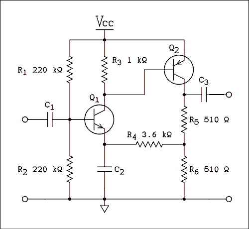
Figure 6.20 Complementary Amplifier Without AC Feedback.
For a verbal description click here.
If Q1 shorts, R4 will protect Q2 from being subjected to excessive base current, as was the case for figure 6.16.In figure 6.20 if Q2 shorts, its collector voltage will become approximately 12 volts, which will increase the voltage applied to the emitter of Q1. The voltage at the base of Q1 is fixed by the voltage divider of R1 and R2. The short in Q2 will pull up the emitter voltage of Q1 to the point of reverse biasing the base-emitter junction of Q1. This will bias Q1 into cutoff.
If R1 opens, both transistors will be driven into cutoff and the voltage at the collector of Q2 will be zero. All other voltages will be what you would expect with both transistors in cutoff.
If R2 opens, both transistors will be in saturation. R4 in the emitter of Q1 will permit Q1 to make it into saturation.
If R3 opens, the effect will be quite noticeable. The collector current of Q1 will be reduced to equal the base current of Q2. This decreases the emitter current of Q1 which will cause the voltage drop across R4 to be reduced. Since the base voltage of Q1 is held nearly constant by the voltage divider of R1 and R2, the emitter voltage will change very little. The voltage at the node where R4, R5 and R6 join will increase. Calculations indicate and tests verify that for the given resistor values, Q2 will be biased into saturation.
If R6 opens, the voltages measured at the terminals of the transistors will change only very little. However, the voltage at the node connecting R4, R5 and R6 will rise from about 3 volts to become equal to the collector voltage of Q2 (about 6 volts). The blame is once again placed on that feedback which does its best to keep the circuit working no matter what is wrong. The circuit will adjust itself to properly bias Q1.
In actuality, both transistors are in cutoff. When a voltmeter is connected to the collector of Q2 it, the voltmeter, provides a load resistance to complete the current path. Both transistors are now conducting very small currents. An additional effect may be that the circuit which was previously dead may come to life (begin to amplify AC signals) when the voltmeter is connected and go dead again when the voltmeter is removed. This may lead one to a false conclusion that there is a loose connection in this part of the circuit.
If R5 opens, the result will be to place Q1 in saturation. The opening of the current path to the collector of Q2 means that the emitter of Q1 must conduct all of the current which is flowing through the resistors to ground. For almost any combination of resistor values this will put Q1 into saturation. When Q1 saturates, Q2 saturates.
Let us now return to a circuit which we looked at earlier, figure 6.13. In section 6.2 we discussed the effects of a short in Q2.
If Q1 shorted, the effect would be to place the emitter and collector resistors in series across the power supply. The collector voltage would be decreased. Q2 will pass this voltage through and decrease the bias on the base of Q3. This may or may not drive Q3 into cutoff. It will depend on the values of the resistors and the power supply voltages.
The following discussion will concern the effect of a total short in Q3. The same effect may well show up if Q1 were to short instead of Q3. Figure 6.13 does not show us what is driving the base of Q1. If it is an emitter follower, the effect would be the same. If it is a higher impedance source, the amplifier may simply go dead.
A total short in Q3 will convert it into a node connecting the emitter of Q2 to the bottom of R4 and the top of R5. While this does place quite a heavy load on Q2, the emitter follower could drive it.
Signals which are injected into the amplifier will come through even with a short in Q3. The gain of 3 which Q3 normally provides will become unity. That is a relatively small change.
The effect on phase shift is the one which will be most noticeable. A common emitter stage such as Q3 in normal operation inverts the input signal. A node connecting some resistors together provides no inversion. The amplifier shown in figure 6.13 is a noninverting amplifier with a gain of 9. When Q3 shorts, the amplifier becomes an inverting amplifier with a gain of 3.
Circuits such as figure 6.13 do not stand in isolation. A circuit such as this will be a small part of a much larger circuit. If the larger circuit has negative feedback, the loss of an inversion will cause this to become positive feedback.
If the feedback is AC coupled, the circuit will oscillate at some unpredictable frequency. If the entire feedback loop is DC coupled, the circuit will simply latch up at one extreme of voltage.
If the larger circuit is an electro-mechanical control system, the system will drive away from the proper point instead of towards it as it should. It will run to the mechanical limit where the limit switches will cause it to stop.
A small loss of gain inside a feedback loop can easily go unnoticed but a change of phase is very noticeable. An amplifier which oscillates or latches up or a control system which drives the wrong way can be a very puzzling situation.
Assume that the circuit of figure 6.13 is part of a sub- assembly which has been removed from a large system and taken to the repair shop. Because the circuit has been removed from its normal signal sources, signal substitution must be used for testing.
The diagram should indicate whether the amplifier unit is inverting or noninverting. The very first test should be to confirm that the phase of the amplifier is correct. If it is incorrect, some very careful testing will be necessary.
Set up the oscilloscope so it is triggered from the signal source. At each stage the scope will show the phase relationship between the input signal and the signal at the test point.
Back to Fun with Transistors.
Back to Fun with TUBES.
Back to Table of Contents.
Back to top.
6.5 Radio Frequency Amplifiers.
Radio frequencies are those that are higher than the audio band. It may surprise you to know that there is actually some overlap. The Omega Navigation system, no longer in operation, used a frequency range from 8 to 12 kHz. With the proper filtering to remove the power line frequency and its harmonics an audio amplifier could be connected to an antenna and some of these transmitters could be heard as they were switched on and off.What distinguishes an RF (Radio Frequency) amplifier from an audio amplifier is that the former contains one or more LC resonant circuits to restrict the band of amplification to a narrow range of frequencies.
Common emitter amplifier.

Figure 6.21 Typical IF Amplifier used in Pocket Radios.
For a verbal description click here.
This circuit is typical of the IF (intermediate frequency) amplifiers found in most transistor sets particularly those 6 transistor pocket radios. Transistors are low impedance devices and the input impedance is especially low. The tuned transformers have been designed to work with transistors operating at a supply voltage of from 9 to 12 volts.The transistor is a triode device and as such has a significant amount of capacitance from input (base) to output (collector). In tubes this problem was solved by adding another grid but this is not possible in a transistor. Therefore an RF amplifier must be neutralized. Note that the Vcc is applied to a tap in the middle of the coil which is not in the exact center. This serves two purposes, one, the impedance between the tap and the near end is lower than the impedance across the entire coil. This prevents the low output impedance of the transistor from lowering the Q of the tuned circuit. Second, by connecting the coil as shown the phase of the voltage at the other end of the coil is 180 degrees out of phase with the voltage at the collector. By connecting a small capacitor, less than 10 pf, from this point back to the base the feedback through the collector to base capacitance of the transistor is canceled by an equal and opposite amount of feedback from the transformer through the capacitor to the base. This is a small ceramic capacitor and its failure is unheard of. If it were to open the amplifier would be likely to oscillate. If it were to short the transistor would be placed in saturation and the circuit would cease to amplify. If the IF strip uses AGC the positive bias is likely to be conducted along the AGC line making it difficult to isolate the problem to a particular stage.
KEEP YOUR SCREWDRIVER OUT OF THE TRANSFORMER ADJUSTING SLUGS!
If the radio or tuner isn't working it isn't because the adjustment screws turned themselves. The cause of the problem is a defective component not because the tuned circuits are mistuned. The only exception to this rule is if an uninformed owner tinkerer tightened up all the loose screws. Also the slugs are made of a material something akin to glass but not as hard. They are held in place by hardened paraffin and will not move easily. If you insert a metal screwdriver and start twisting the result will usually be a broken slug. If you can verify that alignment is necessary the IF transformers in question should be gently warmed under a heat lamp, with a hair dryer, or with a heat gun held a considerable distance away.Open coils and open resistors are more likely than shorted capacitors since the capacitors are usually ceramic with voltage ratings of 50 volts and have a very low probability of failure. DC measurements around the circuit should find the fault. The same formula used in audio amplifiers may be used to calculate the voltages if they are not given.
Grounded or Common Base Amplifier.
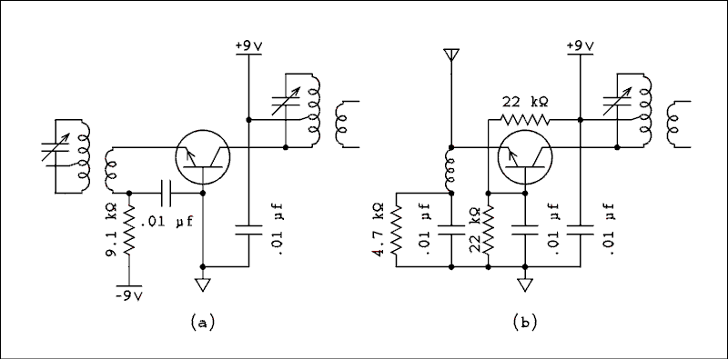
Figure 6.22, Two examples of grounded base amplifiers.
For a verbal description click here.
The transistor is constructed with the base physically between the collector and emitter. If the base could be grounded it would act as an electrostatic shield between the emitter and collector. When the emitter is used as the input element the impedance is quite low typically 25 millivolts divided by the emitter current. As you can see for an emitter current of 1 mA the input impedance is 25 ohms. This is a rather rough approximation and should not be used in the design of impedance matching circuits such as transformers or pi networks.Actually grounding the base is most effective in preventing oscillation even at VHF. The circuit of Figure 6.22 (a) might be found in a short wave receiver or FM tuner. In an S W receiver there most certainly will be band switching which will complicate the schematic. If you examine the diagram carefully you will be able to tease out the basic circuitry.
Figure 6.22 (b) is a circuit often seen in portable FM radios. Because these radios use a single polarity power supply the transistor must be biased with the usual three resistor circuit which means that the base must be grounded through a capacitor rather than directly. The coil is a low Q RF choke which is tuned to the center of the FM band by circuit capacitance. The impedance at the base of a � wave antenna is low which is a match for the input impedance of the amplifier. DC measurements should turn up a fault but connecting a voltmeter lead or oscilloscope probe may well make the circuit start oscillating. It may be necessary to connect a short across the collector coil to kill this oscillation in order to obtain good measurements.
Cascode Amplifier.

Figure 6.23 Cascode Amplifier sometimes found in Ham Radio Projects.
For a verbal description click here.
This circuit is used by amateur builders who don't know or didn't stop to think that a field effect transistor is not constructed like a triode tube. Proper operation of the circuit requires that the upper device have an electrostatic shield between the source and drain. FETs are not constructed in this way. The channel which has the source on one end and the drain on the other is a small bar of N type silicon. The gate is a small dot of P type silicon on one side of the channel. The gate is not physically between source and drain. For the depletion region to serve as an electrostatic shield it would have to occupy the entire cross section of the channel. That would place the FET in total cutoff and it would not function as an amplifier.If you ever have to deal with such a circuit it will most likely come to you as a newly constructed device that has never worked. Slight detuning of the input and output tuned circuits may make it stable enough to use. The circuit is most likely to appear in fixed tuned converters so there is no tracking problem to deal with.
Probably the best cure is to break the "don't modify" rule and change the upper FET to an NPN BJT. I have used circuits of this kind and they are very stable because the grounded base of the BJT does act as an electrostatic shield in the same way as the grid of the triode did in the original tube circuit that the semiconductor version was borrowed from. If a low noise BJT is used the circuit should be just as quiet as it was with the FET. It should actually be quieter because it isn't oscillating.
A modified version of this circuit was used in the FM tuner section of the Heathkit AR-15. Instead of a series coil from the drain of the bottom fet to the source of the top fet the signal was coupled by a combination of magnetic and capacitive coupling. In addition a third winding on this transformer provided neutralization to the circuit. Clearly it took some engineering to make this circuit work well enough for use in a production product. The tuner front end came preassembled and factory aligned in the kit.
Servicing anything more complex than an IF amplifier in an AM receiver is usually beyond the capabilities of small shops and hobbyists and is best left to factory service centers. The reason is that the arrangement of leads and components effects the alignment and neutralization. Replacing a transistor in a VHF amplifier will certainly require the neutralization of the circuit to be readjusted. To do so usually requires a network analyzer which is a very expensive and complex piece of test equipment.
Back to Fun with Transistors.
Back to Fun with TUBES.
Back to Table of Contents.
Back to top.
6.6 Switching Circuits.
Although switching functions have largely been taken over by integrated logic, there are occasions on which a very small amount of switching circuitry is required. On such occasions the designer may elect to use discrete transistor logic.Consider the circuit of figure 6.24. In logic terms This is a noninverting buffer. A "high" input will cause base current to flow in Q1 which will turn it on. When Q1 is on, its collector voltage will be about 0.1 volt ("low") and there will be no bias for the base of Q2. Q2 will be off and its collector voltage will be "high". If the input is "low" there will be no bias for the base of Q1 which will turn it off. With Q1 off, its collector will be "high" and there will be bias for the base of Q2, turning it on. When Q2 is on, its collector will be "low".

Figure 6.24 Discrete Noninverting Buffer.
For a verbal description click here.
If Q1 shorts, its collector will be "low" regardless of the state of the input. Q2 will be off and the output will be "high".If Q2 shorts, its output will be "low" regardless of the state of Q1.
If R2 opens, the circuit would act the same as if Q1 had shorted. If R3 opens, changing logic levels would be observed at the collector of Q1 but Q2 would always be off and there would be a "high" at its collector.
Back to Fun with Transistors.
Back to Fun with TUBES.
Back to Table of Contents.
Back to top.