
Figure 4.1 Simplified Drawing of a BJT With Supply Voltages
For a verbal description click here.
Chapter 4 Transistors as Switches and Amplifiers.
4.1 The Bipolar Junction Transistor (BJT).
4.2 The BJT as a Switch.
4.3 The BJT as an Amplifier.
4.4 The Field Effect Transistor (FET).
4.5 The FET as a Switch.
4.6 The FET as an Amplifier.
4.7 Differential Amplifier.
4.8 Problems.
4.9 Answers to Problems.
Chapter 4.
Transistors as Switches and Amplifiers.
The development of the transistor was the greatest single advancement in electronics since the development of the vacuum tube in the early part of the 20th century. Some people might ask "What about the integrated circuit?" The integrated circuit is just a more compact way of packaging circuitry. In fact, there was a little known attempt in the early 1960s to put vacuum tubes in an integrated package. The information available to the writer indicates that a prototype was actually constructed and tested. The demise of the vacuum tube has relegated this experiment to the dusty back shelves of history. But we digress -- oh yes -- the transistor. Even the very earliest of transistors occupied about 1/100 the volume of the average vacuum tube. Such a large change was bound to start a revolution and it did.Back to Fun with Transistors.
Back to Fun with Tubes.
Back to Table of Contents.
Back to top.
4.1 The Bipolar Junction Transistor (BJT).
The full name of the tiny transistor is quite a mouthful. That is, no doubt, why it is rarely called by that name. Even people who don't know what a transistor looks like know the shortened name "transistor". Non-technical people are unaware that there are two major types of transistors, bipolar junction transistors and field effect transistors. The term "transistor" is too imprecise for our purposes. Instead of using the full name every time, we will use the acronym BJT.A BJT will allow a small current in one circuit loop to control a much larger current (typically 100 times larger) in another circuit loop. The nature of the BJT is such that the current in the second loop may be switched (turned on and off) or varied by an arbitrarily small amount. We will be devoting much space in following sections to the circuits which permit the BJT to be used to control large currents. In this section we will study the internal physics of the BJT and try to understand how it does what it does.
A simplified cross-section of a BJT is shown in Figure 4.1. A bipolar junction transistor consists of three layers of alternating semiconductor type. These three layers have been given the names emitter, base and collector.
Figure 4.1 Simplified Drawing of a BJT With Supply Voltages
For a verbal description click here.
BJTs may be manufactured in either of two forms. In one form the emitter is P type semiconductor, the base is N type semiconductor and the collector is P type semiconductor. Such transistors are referred to as PNP transistors. In the other form the emitter is N type semiconductor, the base is P type semiconductor and the collector is N type semiconductor. Such transistors are referred to as NPN transistors. (The designation NPN or PNP informs the reader that the transistor is a bipolar junction type and the term NPN transistor is precise.) In the example of Figure 4.1 the transistor is an NPN type which means that the emitter is N type semiconductor, the base is P type semiconductor and the collector is N type semiconductor.The connection of the battery on the left is such as to forward bias the P-N junction between the emitter and base. The voltage drop across the emitter-base junction is about 0.6 volts. (We used 0.7 volts in rectifier circuits because the current is fairly high. In the base circuit of a BJT the currents are fairly small, typically a few tens of microamperes and the voltage drop is more typically 0.6 volts.) The collector supply voltage, VCC may be anywhere between 5 volts and the maximum the transistor will stand. With the base at +0.6 volts and the collector at more than +5 volts, the base-collector junction is reverse biased.
The forward biased emitter-base junction causes majority carriers to move across the junction. These charge carriers become minority carriers as soon as they cross the junction. Minority carriers do not immediately combine with majority carriers but will travel a short distance until statistics catch up with them and recombination occurs. The average distance a minority carrier can cover is called the mean free path. In a real transistor the width of the base region is less than the mean free path of a minority carrier in the base. That means that most of the minority carriers which are injected into the base region will make it across the base without being recombined with majority carriers from the base. As soon as a minority carrier exits the base and enters the collector, it is again a majority carrier. Majority carriers which are injected into the collector will constitute a collector current. That collector current originated in the emitter and is controlled by the base current.
In the specific case of the NPN transistor shown in Figure 4.1 the base supply voltage VBB will cause a base current to flow into the base. That will cause holes from the base to cross into the emitter and electrons from the emitter to cross into the base. The holes from the base will simply recombine with electrons in the emitter. Some electrons from the emitter will flow out through the base connection and back to VBB but most of the electrons which cross the emitter-base junction will continue on to cross the base-collector junction. Thus there are electrons originating in the emitter region and ending up in the collector region.
If the base current is increased, the number of charge carriers injected into the base will be increased and so will the number of carriers injected into the collector. More base current means more collector current. Less base current means less collector current. The animation below shows this. If the base current is shut off, the collector current will cease to flow. The collector current is typically 100 times larger than the base current.
Figure 4.1a Animation showing holes and electrons in a BJT.
For a verbal description click here.
If a PNP transistor were to be used in the circuit of Figure 4.1, it would be necessary to reverse both batteries. The discussion above will apply to a PNP transistor, the only changes to be made are to change every occurrence of "electron" to "hole" and "hole" to "electron". All references to majority and minority carriers remain as they are.Figure 4.2 is a repeat of Figure 4.1 but with the schematic symbol for an NPN transistor instead of the representation of the transistor's innards. We will now define a transistor parameter. It is called the forward DC current gain. It is assigned the symbol beta and is
beta = IC / IB (4.1) where IC is the DC collector current and IB is the DC base current of the transistor. Equation 4.1 is a definition and so cannot be derived.

Figure 4.2 Schematic of a Properly Biased NPN Transistor.
For a verbal description click here.
By applying Kirchhoff's and Ohm's laws to the circuit of Figure 4.2 it is possible to write some other equations. Summing currents we haveIE = IC + IB (4.2) where IE is the emitter current. Summing voltages around the base loop we haveVBB = IB RB + VBE (4.3) where VBE is the base to emitter voltage drop, which is approximately 0.6 volts. If we substitute VBE = 0.6 v and rearrange equation 4.3 we haveIB = (VBB - 0.6 v) / RB (4.4) In the collector loop we can writeVCC = IC RC + VCE (4.5) where VCE is the voltage between collector and emitter. In a great many circuits VCE is taken as the output voltage of the transistor circuit. Rearranging equation 4.5 we haveVCE = VCC - IC RC (4.6) If we combine equations 4.1, 4.4 and 4.6 we haveVCE = VCC - beta RC (VBB - 0.6 v) / RB (4.7) VCE can never, repeat NEVER, change sign. The absolute value of VCC must always be greater than the absolute value of VCE in equation 4.7. VCE can never exceed VCC because to do so would require that the term on the right in equation 4.7 undergo a change of sign. That cannot happen in the real world. Because the base-emitter junction is a P-N junction diode, if VBB becomes less than 0.6 volts, the base current will simply stop, not reverse. VCE will be equal to VCC.Within the limits 0 to VCC notice that if VBB is decreased, VCE is increased and visa versa. These are common emitter equations and may not apply to all circuits employing bipolar transistors.
The important thing about these seven equations is to understand how they were obtained. If you do not understand how these equations were obtained it is guaranteed that the rest of this chapter will be Greek to you.
Back to Fun with Transistors.
Back to Fun with Tubes.
Back to Table of Contents.
Back to top.
4.2 The BJT as a Switch.
As mentioned above if the base current is removed from a transistor, the collector current will become similar to the reverse current in a diode, (too small to measure). Thus if a small current is turned on and off in the base of a BJT, the collector current will be turned on and off. Because the collector current is much larger than the base current, a low power circuit can be made to turn a high power device on and off. An excellent example of this is an indicator light.

Figure 4.3 BJT Switch Turns Light On and Off
For a verbal description click here.
Figure 4.3 shows how a transistor can be used to turn a light on and off. It is very common in both consumer and laboratory equipment for a light to come on to indicate that a particular function has been activated. The input terminals on the left connect to what will be referred to as the driving source. The driving source is not capable of delivering enough current to light the lamp. This low power circuit will deliver a voltage when the light is to be on and no (or very little) voltage when the light is to be off.An ideal switch has infinite resistance when it is open and zero resistance when it is closed. The BJT is quite close to being ideal in the open (off) condition but in the closed (on) condition it is not quite perfect. The on condition is known as saturation and is the condition wherein the collector current is as large as it can be. When a transistor is in saturation VCE is about 0.1 or 0.2 volts.
When a BJT is in saturation, most of the power supply voltage will appear across the load (device being switched on and off) and so the current through the load is
ISAT = (VCC - VCESAT) / RL (4.8) where VCC is the power supply voltage, RL is the load resistance and 0.1 v < VCESAT < 0.2 volts.
Example 4.1.
A lamp having a resistance of 22 ohms is to be switched by a BJT. The power supply voltage is 5 volts and the collector saturation voltage is 0.1 volts. What is the saturation current of the transistor? See Figure 4.3.Solution:
ISAT = (5 v - 0.1 v) / 22 ohms = 223 mATrouble can develop in switching circuits if the transistor is not in saturation. To place a transistor in saturation it is necessary to supply more base current than is needed to just barely place the transistor in saturation. To be absolutely certain that the transistor is in saturation, the base current should be at least twice that required to just barely saturate the transistor. It will not do any damage if the base current is larger than that required for saturation. The collector current cannot be any greater than the saturation current.
Example 4.2.
Using the same conditions from example 4.1, what is the minimum base current required to place the transistor in saturation if beta is 80?Solution:
IBMIN = ISAT / beta = 223 mA / 80 = 2.79 mAThe resistor in the base circuit must be properly selected so as to cause the base current to be large enough to place the transistor in saturation. On the other extreme the driving source will have a practical limit to how much current it will supply. If there were no limit, the load could be connected to the source and the switching transistor would not be needed.
Example 4.3.
Continuing with examples 4.1 and 4.2, what is the range of resistance for RB if the driving source can supply a maximum of 12 mA at a voltage of 5 volts. What should the resistance be to give a saturation safety factor of 2.5?Solution:
In example 4.2 the minimum base current was calculated to be 2.79 mA. The maximum base current is the maximum which the driving source can supply, which is given as 12 mA. Solving equation 4.4 for RB we haveRB = (VBB - 0.6 v) / IB
RBMIN = (5 v - 0.6 v) / 12 mA = 367 ohms.
RBMAX = (5 v - 0.6 v) / 2.79 mA = 1.58 k ohms.
Since the minimum base current for saturation is 2.79 mA
a safety factor of 2.5 calls for a base current of 6.98
mA. RB = (5 v - 0.6 v) / 6.98 mA = 630 ohms.
A 620 ohms standard value resistor would be used.Another consideration in switching transistor circuits is whether the transistor will be turned off when it is supposed to be off. As long as the voltage of the driving source goes below about 0.6 volts, the transistor will most likely be turned off. But some driving sources do not go below 0.6 volts and the transistor may not be completely turned off.
Example 4.4.
In Figure 4.3 it is now assumed that VCC is 5 volts, the resistance of the lamp is 22 ohms, the resistance of RB is 620 ohms and the beta of the transistor is 80. The driving source has an "on" voltage of 5 volts. (a) If its "off" voltage is 0.2 volts, is the transistor off? If not, what is the collector current? (b) If the driving source has an "off" voltage of 1.0 volts, is the transistor off? If not, what is the collector current?Solution:
(a) The driving source has an "off" voltage of 0.2 volts. That is less than the 0.6 volt breakdown of the base-emitter junction. There will be no base current and so there will be no collector current. The transistor switch will be off.
(b) If the "off" voltage of the driving source is 1 volt there will be some base current. The base current will be IB = (1 v - 0.6 v) / 620 ohms = 0.645 mA; the collector current will be 80 x 0.645 mA = 51.6 mA. Although they are not asked for in the original example we will calculate the drop across the load and VCE to give a complete illustration of this type of problem. The drop across the load is IC RL = 51.6 mA x 22 ohms = 1.14 volts. VCE is VCC - VL = 5 v - 1.14 v = 3.86 volts.As you can see in the above example the transistor is "mostly" off. The lamp would glow slightly. An operator might be confused and become unsure as to whether a particular function is engaged or not. In something such as a nuclear power plant such confusion could be the difference between safe and unsafe operation. It is highly undesirable for indicator lamps to be partially on when they are supposed to be off.
Figure 4.4 shows a circuit which will overcome the problem of a driving source which will not go to zero for the off state.

Figure 4.4 Switching Circuit for Non-zero Driving Sources
For a verbal description click here.
The procedure for solving this circuit is as follows.
- Assume that there is no load on the voltage divider in the base circuit and see if the transistor will be turned on or not. If the calculated voltage exceeds 0.6 volts, the transistor is at least part way on. If the voltage is less than 0.6 volts the transistor is off.
- To calculate the base current in the "on" state assume that VBE is 0.6 volts and calculate the current through R2 (the voltage across R2 will be 0.6 volts).
- Calculate the current through R1 assuming VBE to be 0.6 volts.
- The current through R1 will split. Some will go through R2 and the rest will go into the base of the transistor. To obtain the base current subtract the R2 current from the R1 current.
For those who would rather memorize an equation it is
IB = (VDSON - 0.6 v) / R1 - 0.6 v / R2 (4.9) where VDSON is the on voltage of the driving source. It should be pointed out and emphasized that VBE for a good (not burned out) BJT can never exceed about 0.6 or 0.7 volts. If it does in a calculation, something has been neglected but no damage is done. If VBE exceeds 0.7 volts in the real world, the BJT is burned out. If it wasn't before, it is now.
Example 4.5
For the values given in Figure 4.4 will a driving source which has an on voltage of 5 volts and an off voltage of 1 volt turn the BJT switch on and off?Solution:
For the off state VBE = 1 v x 1 k ohms / (5.6 k ohms + 1 k ohms) = 0.15 v; the BJT switch is off. For the on state VBE = 5 v x 1 k ohms / (5.6 k ohms + 1 k ohms) = 0.76 v; there will be base current. Calculating the amount of base currentIB = VDSON - 0.6 v) / R1 - 0.6 v / R2 = 4.4 v / 5.6 k ohms - 0.6 v / 1 k ohm = 0.186 mA
The base current required to turn the switch on is IB = IC / beta and IC = RC / VCC = 12 v / 150 ohms = 80 mA, IB = 80 mA / 100 = 0.8 mA. With 0.8 mA required and 0.186 mA supplied, there is insufficient base current to turn the BJT switch on.
Example 4.6
Will a driving source of 10 volts turn the BJT on in Figure 4.4?Solution:
We know from example 4.5 that 5 volts is enough to slightly forward bias the base-emitter junction and so we do not need to test to see if 10 volts will do it. Calculating IB givesBJT switches are used whenever a device such as a microprocessor needs to switch the current to any device which draws more current than the microprocessor can supply. Devices which may be switched include lamps, relays, buzzers and digital displays.IB = (10 v - 0.6 v) / 5.6 k ohms - 0.6 v / 1 k ohm = 1.08 mA.
In example 4.5 we saw that 0.8 mA was required to turn the BJT on and we have 1.08 mA. The BJT is on.
Back to Fun with Transistors.
Back to Fun with Tubes.
Back to Table of Contents.
Back to top.
4.3 The BJT as an Amplifier.
An amplifier is any sort of device which will increase the magnitude of a signal. An amplifier may increase the magnitude of the voltage, current or both but to qualify as a true amplifier it must increase the power of a signal. A transformer can be used to increase the voltage of a signal, but there is no increase in power and a transformer is not an amplifier.To characterize an amplifier completely it is necessary to know four things about it. They are
These characteristics are called the four-terminal network parameters.
- the relationship between the input voltage and the input current,
- the relationship between the output voltage and the output current,
- a relationship showing how the output is affected by the input, and
- a relationship showing how the input is affected by the output.
There are three groups of parameters, the impedance parameters, the admittance parameters and the hybrid parameters. All four of the impedance parameters have units of ohms and all four of the admittance parameters have units of ohms-1. The hybrid parameters are a mix of units.

Figure 4.5 Generalized Four-terminal Network
For a verbal description click here.
Figure 4.5 shows a generalized four-terminal network. The open circuit impedance parameters are as follows."What has all of this to do with transistors?" A transistor can be treated as a four-terminal network. "Hold on now, you said a transistor has three terminals, emitter, base and collector, I remember that!" Correct. We will use one of the terminals twice so as to use four-terminal network parameters on a BJT.
- Input Impedance Z11 = V1 / I1 with I2 = 0
- Output Impedance Z22 = V2 / I2 with I1 = 0
- Forward Transfer Impedance Z12 = V2 / I1 I2 = 0
- Reverse Transfer Impedance Z21 = V1 / I2 I1 = 0
Let us apply the hybrid parameters to the common emitter configuration. That means that the input is applied between the base and emitter and the output is taken between the collector and emitter as indicated in Figure 4.6a.
In the equations to follow all of the voltages and currents are AC small signal. Small signal means that the AC voltages are small enough so that the natural nonlinearities of P-N junctions are not significant and the I-V characteristics "look" linear. This is not an unrealistic condition. All amplifier transistors must be used in this way to avoid signal distortion. Distortion is any unwanted alteration of the signal.
The small-signal common-emitter hybrid parameters for the BJT are as follows.
The short-circuit input impedance.
hie = vbe / ib with vce = 0 (4.10) The open-circuit output admittance.hoe = ic / vce with ib = 0 (4.11) The short-circuit forward current transfer ratio.hfe = ic / ib with vce = 0 (4.12) The open-circuit reverse voltage transfer ratio.hre = vbe / vce with ib = 0 <(4.13) Just in case you are wondering, hre is measured by injecting a signal at the collector and making a measurement at the base. These parameters are all definitions.

Figure 4.6 (a) BJT and (b) Four-terminal Equivalent Circuit.
For a verbal description click here.
The hybrid parameters give rise to the equivalent circuit of Figure 4.6b. This circuit takes the place of the transistor and is considered to be equivalent to it. The parameter hie is the input resistance. It is connected in series with the voltage generator which represents hre. The presence of hre indicates that a small amount of the output voltage is fed back into the base-emitter loop. In the collector-emitter loop a resistor representing hoe and a current source representing hfe are connected in parallel. Although hoe is expressed as a conductance, it is the reciprocal of the output resistance of the transistor. The current produced by the current source hfe is equal to hfe times the current in the base loop.A generator may be connected, (in thought), to the base- emitter side of the equivalent circuit and a load resistance connected to the collector-emitter side. Equations may then be derived for such things as the input impedance, the output impedance and the gain. These equations are indeed complex. Advancing technology has saved us from having to deal with these equations.
The voltage feedback which is represented by hre is caused by the electric field within the transistor which is produced by the collector-to-emitter voltage. This field affects the concentration of charge carriers within the base and causes the forward voltage drop across the base-emitter junction (VBE) to be affected by the magnitude of VCE. The same electric field causes the collector current to increase as VCE increases. The value of hoe is the slope of the graph of IC versus VCE. Modern transistor design has overcome both of these problems to a very large extent. The amount of output voltage which is fed back to the input side is negligible in modern transistors and hre can be neglected and removed from the equivalent circuit. With modern transistors the graph of IC versus VCE is a horizontal line for voltages above about 1.5 volts. A horizontal line has a slope of zero and if hoe is zero, the output resistance is infinity. An infinite output resistance means that the resistor representing hoe may be removed from the circuit.

Figure 4.7 Simplified Equivalent Circuit.
For a verbal description click here.
The simplified equivalent circuit is shown in Figure 4.7. The equivalent circuit consists of the resistor labeled hie and the current source labeled ib> hfe. To make use of this circuit we must connect a couple of things to it. A Thevenin's equivalent circuit of a generator is connected to the B and E terminals. A load resistor is connected to the C and E terminals. We will use this circuit to derive the equations for gain and input impedance.The current in the first loop is simply,
The output voltage is, ib = vbe / hie (4.14)
vce = - hfe ib RL (4.15) The minus sign in equation 4.15 arises from the fact that the current in the current source is flowing downward and so it is flowing upward in the load resistor. If we now substitute equation 4.14 into equation 4.15 and divide by vbe we obtain,vce / vbe = - (hfe RL ) / hie (4.16) If we define the voltage gain as AV = vce / vbe then we haveAV = - (hfe RL ) / hie (4.17) The input impedance of a common emitter amplifier is equal to Hie. The output impedance is virtually infinite.Example 4.7
A BJT has the following parameters, hfe = 90 and hie = 4 k ohms. If this transistor is placed in a circuit where the load resistance is 4.7 k ohms, what is the voltage gain of the circuit?Solution:
AV = - (hfe RL ) / hie = - ( 90 x 4.7 k ohms ) / ( 4 k ohms ) = 106The solution to example 4.7 indicates that the amplifier in question will have an output voltage 106 times as large as its input voltage and the phase of the output signal will be inverted. 180 degrees phase shift.
Biasing the Bipolar Transistor.
The BJT is normally used to amplify small AC signals but it won't do anything unless it is provided with the proper DC voltages and currents. The process of providing the DC values is called biasing. One way to bias a transistor is as shown in Figure 4.2. The combination of VBB and RB will provide a constant DC current to the base. The collector current should be adjusted such that 1/2 of VCC is dropped across RC. VCE will also be 1/2 of VCC. This condition permits the AC output signal to be as large as it can possibly be. The collector voltage can "swing" from 0 to VCC. This type of biasing is never used in practical circuits because the collector current depends on the value of the DC beta of the transistor. The value of beta changes with temperature and is different for different transistors even of the same type number.

Figure 4.8 Practical Audio Frequency Amplifier.
For a verbal description click here.
A complete practical one-stage audio frequency amplifier is shown in Figure 4.8. Approximately 2 volts DC are dropped across the emitter resistor which leaves a 10 volt range for VCE (2 volts to 12 volts). The static collector voltage is halfway between 2 and 12, which is 7 volts. The voltage at the base is approximately 2.6 volts. Capacitor C1 is necessary to prevent this voltage from interfering with the operation of or possibly even damaging the device which is to provide the signal to the amplifier. C3 blocks the DC at the collector from reaching the circuits or devices which may be connected to the output of the amplifier. R5 provides a charging path for C3 to make sure that there is no DC voltage present at the output even though there is no other load connected. Remember back in chapter 2 when we were talking about mixtures of AC and DC? Well, here it is. The RC networks are used just as described to pass the AC while blocking the DC.The purpose of C2 requires a bit more explanation. If C2 were not present, the gain of the amplifier would be considerably reduced. It works this way. When the input signal goes positive, the base current increases and so does the emitter current. That increases the voltage drop across the emitter resistor and reduces the effect of the increasing signal. The effect of the signal could not be completely canceled out because, if the change in emitter current were completely canceled out, there would be no change in emitter current to cancel out the change in base current. The effect of the changing input signal is considerably reduced, which considerably reduces the gain of the circuit. Connecting C2 from the emitter to ground will prevent rapid changes in the emitter voltage and so the input signal will not have its effect reduced by any changes in the emitter voltage. The process of reducing the effective gain by removing the emitter bypass capacitor C2 is called emitter degeneration and, as we will learn in the next chapter, is not necessarily a bad thing.
Operating Point Stability
The set of conditions, IC, VCE, etc., are referred to collectively as the operating point. The operating point of a transistor must be stabilized against two types of changes. 1) The temperature can change and the value of beta is very temperature dependent. 2) Changing transistors, transistors can and do burn out and have to be replaced. The replacement most likely will not have the same value of beta as the original unit. There is no guarantee that a circuit will always be operated at room temperature. Air conditioning and heating systems can break down; portable devices can be carried outside on a summer or winter day. A device which fails to operate if the temperature gets above 85degrees or below 65degrees will not be very useful. If a transistor burns out it must be replaced to restore operation. Even if the replacement transistor has the same number as the original transistor, its beta may differ by as much as 30% from the original. If the circuit is not properly designed, the circuit may not work following the replacement of a defective transistor.If the circuit of Figure 4.2 were used as an amplifier (and it could be) it would suffer from both problems described above. The circuit of Figure 4.8 does not suffer from these problems and here is why. The base current is small compared to the current flowing down through R1 and R2. The voltage divider which is constituted by R1 and R2 is lightly loaded and its output voltage will change only slightly as the base current changes. Suppose that the collector current tries to increase due to a temperature or a transistor change. The emitter current is IC + IB and IB is very much less than IC; therefore, IE is approximately equal to IC. As IC goes so goes IE. IE is trying to increase which will increase the voltage drop across RE which, in turn, will increase the voltage at the emitter. The voltage divider of R1 and R2 is holding the voltage at the base almost constant. An increase of emitter voltage while the base voltage is held constant will cause the forward bias on the base-emitter junction to be decreased and, therefore, decrease the base current. Remember we started out with the emitter current trying to increase which led to a decrease in base current. A decrease in base current will counteract the original increase in collector (emitter) current and the increase will not be as great as it would otherwise be. In fact, the emitter current will change only very slightly. If the collector (emitter) current tries to decrease, the voltage across RE will decrease, decreasing the emitter voltage while the base voltage is held constant. This increases the forward bias on the B-E junction and increases the base current which counteracts the decrease in collector (emitter) current.
If you were to set up the circuits of Figures 4.2 and 4.8 and put meters in the circuit to monitor the base and collector currents, you could see things happen. In the case of Figure 4.2 if heat were applied to the transistor the collector current would rise very rapidly. In the case of Figure 4.8 the collector current would change very slightly and the base current would drop off drastically. If the transistor were cooled, the currents would change in the opposite direction. A transistor with a higher beta will result in a larger collector current in the circuit of Figure 4.2 and a smaller base current in Figure 4.8.
The circuit of Figure 4.2 is called constant current biasing. It is never used in analog (as opposed to switching) circuits. The circuit of Figure 4.8 is called constant voltage biasing and it - or a variation of it - is used in all transistor circuits, including the internal circuitry of integrated circuits.
Circuit Analysis.
The circuit of Figure 4.8 is much easier to analyze if the voltage divider is replaced by its Thevenin's equivalent circuit as shown in Figure 4.9. Capacitors have been omitted because this is a DC analysis and capacitors are open circuits for DC. The values of VBB and RB are given by these equationsVBB = VCC R2 / (R1 + R2) (4.18) and
RB = (R1 R2) / (R1 + R2) (4.19) where R1 and R2 are the original base resistors as shown in Figure 4.8.

Figure 4.9 Thevenin's Equivalent Circuit Replaces R1 and R2
For a verbal description click here.
If equations 4.18 and 4.19 seem to have "come out of the blue," you need to review the section on Thevenin's equivalent circuit (section 1.3 pages 41 to 46).We will now write the loop equations for the circuit of Figure 4.9. Summing voltages in the base loop gives
VBB = RB IB + VBE + RE (IB + IC) (4.20) The voltage drop across RE (R4 in Figure 4.8) is IE RE but IE = IB + IC. The base current is given by
IB = IC / beta (4.21) Substituting equation 4.21 into equation 4.20 and solving for IC gives
IC = beta (VBB - VBE) / (RB + RE (1 + beta)) (4.22) If beta is greater than 50 an error of less than 2% will be introduced by letting the (1 + beta) term in the denominator equal beta. Making this substitution and dividing through by beta we have
IC = (VBB - VBE) / (RE + RB / beta) (4.23) Equation 4.23 is probably the best one to use to calculate the collector current of a constant voltage biased BJT.
It is possible to make a further approximation but it must be applied with great care. In the denominator of equation 4.23 RB / beta may be much less than RE. If this is true the following equation may be used.
IC = (VBB - VBE) / RE if and only if RB / beta << RE. (4.24)
Example 4.8
Calculate the values of VBB and RB for the circuit of Figure 4.8.Solution:
VBB is the unloaded output of the voltage divider consisting of R1 and R2VBB = VCC R2 / (R1 + R2) = 12 v x 6.8 k ohms / (22 k ohms + 6.8 k ohms) = 2.83 v
RB is the parallel combination of R1 and R2
RB = R1 R2 / (R1 + R2) = 22 k ohms x 6.8 k ohms / (22 k ohms + 6.8 k ohms) = 5.19 k ohms
Example 4.9
If the transistor in Figure 4.8 has a beta of 150, what is the collector current?Solution:
Which equation should we use? Equation 4.22 is the most exact form but the difference between beta and beta + 1 is only 0.66%. We might use equation 4.24 but that one is usually used only when beta is not given and a typical value must be assumed. We will use equation 4.23.IC = 2.83 v - 0.6 v / (1.8 k ohms + 5.19 k ohms / 150) = 2.23 v / (1.8 k ohms + 0.03 k ohms) = 1.22 mA.
If equation 4.24 had been used the error would have only been 1.67%, which is well within acceptable limits. Perhaps another example will illustrate when equation 4.24 should not be used.
Example 4.10
In a circuit similar to Figure 4.8 VCC = 15 v, R1 = 100 K ohms, R2 = 47 k ohms, R3 = 4.7 k ohms, R4 = 3.3 k ohms and beta = 50. What is the collector current?Solution:
Since beta = 50 this is a borderline case for the 2% rule but we will ignore beta + 1 and use equation 4.23. VBB = 15 v x 47 k ohms / (100 k ohms + 47 k ohms) = 4.80 v and RB = 100 k ohms x 47 k ohms / (100 k ohms + 47 k ohms) = 32.0 k ohms.IC = 4.80 v - 0.6 v / (3.3 k ohms + 32.0 k ohms / 50) = 4.20 v / (3.3 k ohms + 0.64 k ohms) = 1.07 mA.
The Common Collector (Emitter-follower) Amplifier.
If the collector of a BJT is placed at AC ground potential while the input signal is applied between ground and base and the output signal is taken between ground and emitter, the collector is common to input and output. Such an amplifier is a common collector configuration but is commonly known as an emitter-follower. An AC coupled emitter-follower is shown in Figure 4.10.

Figure 4.10 AC Coupled Emitter-follower.
For a verbal description click here.
The reason it is called an emitter-follower is because of that nearly constant 0.6 volt drop from base to emitter. How ever the base voltage may change, the emitter voltage is following along only 0.6 volts behind. To put it more precisely, for an NPN transistor the emitter voltage is 0.6 volts less then the base voltage. For a PNP transistor the emitter voltage is 0.6 volts greater than the base voltage. That 0.6 volts may not be important in the circuit of Figure 4.10 but in a DC coupled emitter-follower it may be very important.The AC gain of an emitter-follower may be derived using the familiar common emitter parameters by drawing the equivalent circuit as in Figure 4.11. This circuit is a little difficult to follow (pun fully intended) and so the wires have been untangled in Figure 4.12. In equivalent circuits it is customary to omit DC biasing and capacitors because they add nothing to the AC circuit.

Figure 4.11 Common Collector Equivalent Circuit.
For a verbal description click here.
Figure 4.12 Figure 4.11 with Wires Untangled.
For a verbal description click here.

Writing a loop equation around the outside loop givesvin = ib hie + vo. (4.25) We will make the approximation that the base current ib is much less than the collector current ic, and the emitter current will be considered equal to the collector current. The current flowing through RL is the collector current hfeib and we have
vo = ib hfe RL. (4.26) If we solve equations 4.25 and 4.26 for ib and set them equal we have
vo / (hfe RL) = (vin - vo) / hie (4.27) Solving this equation for vo / vin and remembering that voltage gain is defined as vo / vin we have
AV = hfe RL / (hie + hfe RL) (4.28)
Example 4.11.
A BJT has the following parameters, hie = 4 k ohms and hfe = 100. In an emitter-follower with a load (emitter) resistor of 1 k ohms, what is the voltage gain?Solution:
AV = hfe RL / (hie + hfe RL) = 100 x 1 k ohm / (4 k ohms + 100 x 1 k ohm) = 0.962The voltage gain of an emitter-follower is always slightly less than one. You may be wondering what use is an amplifier which slightly reduces the amplitude of the input signal. An emitter-follower has current gain. The current gain is equal to beta. For example, if you have a generator which can only supply 1 mA and you need to drive a load which requires 100 mA, an emitter-follower employing a BJT with a beta (or hfe) greater than 100 will allow the generator to drive the load provided there are no other losses in the circuit.Input Resistance.
The input resistance of an emitter-follower isRin = vin / ib (4.29) If we rearrange equation 4.26 we have
vo / ib = hfe RL (4.30) Because the gain of an emitter-follower is approximately unity, vo = vin. Combining this approximation with equations 4.29 and 4.30 we have
Rin = hfe RL (4.31) The value of RL is the parallel combination of all resistances connected from the emitter to ground.
Example 4.12.
In the circuit of Figure 4.13 an emitter-follower is being used to drive an 8 ohm speaker. If R1 = R2 = 390 ohms, R3 = 15 ohms, beta = hfe = 75 and hie = 5 ohms, what are (a) the voltage gain and (b) the input resistance?

Figure 4.13 Emitter-follower Driving a Speaker
For a verbal description click here.
Solution:
(a) The gain is given by equation 4.28. RL in this equation is the parallel combination of R3 and the 8 ohm speaker which is 5.22 ohms.AV = hfe RL / (hie + hfe RL = 75 x 5.22 ohms / (5 ohms + 75 x 5.22 ohms) = 0.987
(b) The input resistance is the parallel combination of the two 390 ohm resistors in the base circuit and the input resistance of the emitter-follower. The input resistance of the emitter-follower is given by equation 4.31.
Rin = hfe RL = 75 x 5.22 = 392 ohms
The total input resistance is the parallel combination of 390 ohms, 390 ohms and 392 ohms which is 130 ohms
Resistances in Parallel.
Some of you may be puzzled over why resistors are being treated as if they are connected in parallel when they are not connected to the same point in the circuit. If you are not puzzled, you may skip this section.For example, the speaker and the 15 ohm resistor R3 have been treated as if they are in parallel when it is obvious that there is a capacitor connected between them. We are talking about AC not DC. The job of the capacitor is to block DC and pass AC to the speaker. The value of the capacitor has been chosen such that its reactance is small at the lowest frequency to be passed to the speaker. The capacitor is essentially a short circuit for AC. When the capacitor is replaced by a short circuit the speaker and the 15 ohm resistor are in parallel.
The two 390 ohm resistors in the base appear more like they are in series than in parallel. The AC signal is applied to the junction of the two resistors. One of the resistors goes to ground and the other one goes to the power supply (VCC). Within the power supply is a large capacitor connected from VCC to ground, or a voltage regulator, most likely both. For AC there is a short circuit connected from VCC to ground, which means that connecting a resistor to VCC is the same as connecting it to ground as far as AC is concerned. The input resistance of the transistor appears from base to ground and so is in parallel with the resistors in the base circuit.
Output Resistance.
To determine the output resistance of an emitter- follower we rearrange the equivalent circuit of Figure 4.12 and redraw it in Figure 4.14.

Figure 4.14 Measuring Output Resistance of Emitter-follower.
For a verbal description click here.
The generator has been removed from the input and replaced by its internal resistance Rg. The load resistor has been removed and a generator has been connected to the output. The purpose of this is to apply a known voltage to the output and see how much current flows.This can be done in the laboratory if care is taken not to drive the transistor into nonlinear regions of its I-V characteristic.
Summing the voltage drops around the outside loop gives
ib (Rg + hie) = V. (4.32) The current flowing in the generator is
I = ib (hfe + 1). (4.33) Eliminating ib between equations 4.32 and 4.33 and rearranging yields
V / I = (Rg + hie) / (hfe + 1) (4.34) Since RO = V / I we have
RO = (Rg + hie) / (hfe + 1) (4.35)
Example 4.13.
In the circuit of Figure 4.13 calculate the output resistance which is effectively connected across the speaker. The output resistance of the generator is 50 ohms.Solution:
The output resistance at the emitter of the transistor is given by equation 4.35. Rg must be the parallel combination of the generator resistance and the two resistors in the base circuit, 50 ohms in parallel with two 390 ohm resistors, which is 39.8 ohmsRO = (Rg + hie) / (hfe + 1) = (39.8 ohms + 5 ohms) / (75 + 1) = 0.589 ohms
The true output resistance is RO in parallel with 15 ohms but it isn't going to make much difference.
Rout = 15 ohms x 0.589 ohms / (15 ohms + 0.589 ohms) = 0.567 ohms.
Determining Transistor Parameters.
Transistor parameters may be found in a data sheet for the particular transistor or in a transistor data book. Data sheets for individual transistors may be obtained from the manufacturer often free of charge or for a nominal fee. These data sheets give all of the information you could possibly want. Data sheets give a range of values for each parameter. Whether you use an average value or the minimum value will depend on what you are trying to do.Most data books do not give a value for hie at all. They usually give a range of values for the current gain. For audio frequencies the values of beta and hfe are the same. It is unusual for a data book to give a value of hfe at high frequencies.
If you need to know the value of hie and you can't find it anywhere you can estimate it. Hie = 25 mv / IB. Since IB = IC / beta hie can be estimated as
Hie = 25 mv x beta / IC (4.36)
Back to Fun with Transistors.
Back to Fun with Tubes.
Back to Table of Contents.
Back to top.
4.4 The Field Effect Transistor (FET).
There are two classes of field effect transistors, junction field effect transistors, JFETs, and metal oxide semiconductor field effect transistor, MOSFETs. We will begin with JFETs.The Junction Field Effect Transistor.
Figure 4.15 Junction Field Effect Transistor.
For a verbal description click here.
Figure 4.15 shows an N channel junction field effect transistor (JFET). If a battery is connected to the ends of the channel, (source and drain) current will flow as if it were a resistor. Like any other resistance device the resistance will depend on the length and cross-section area of the block of semiconductor material.It is the cross-section area which is important in the JFET. If the gate to channel junction is reverse-biased the depletion region will grow outward from the gate as shown in Figure 4.16. As the depletion region grows larger the conduction cross-section area is decreased. The depletion region does not conduct current. As the reverse bias voltage on the gate-channel junction is increased, the resistance of the channel is increased. At comparatively large gate to channel voltages (about 10 volts) the channel resistance is approaching infinity. At a gate to channel voltage of zero the channel resistance is low, a typical value being 100 ohms.
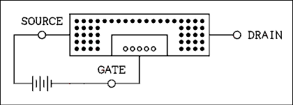
Figure 4.16 JFET with Reverse Bias on the Gate.
For a verbal description click here.
Figure 4.17 JFET Showing Pinch-off Effect.
For a verbal description click here.
When a battery is connected across the ends of the channel, another effect becomes evident. Because the gate reduces the channel cross-section area, the resistance in the region of the gate is increased and most of the voltage which is applied will be dropped across the region occupied by the gate. This voltage drop causes the channel near the top of the gate (Figure 4.17) to be more positive than the channel near the bottom of the gate. The net voltage across the gate-channel junction is greater at the top than it is at the bottom. Hence, the depletion region will be wider at the top of the gate than it is at the bottom, as shown in Figure 4.17. As the voltage applied to the ends of the channel is increased, this effect is increased until the channel becomes a constant current device. The channel does not become a negative resistance device (current decreases as voltage increases). The voltage at which the channel changes from a resistive device to a constant current device is called the pinch-off voltage.
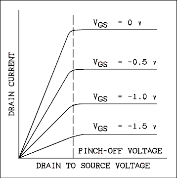
Figure 4.18 Drain Characteristics of a typical FET.
For a verbal description click here.
Figure 4.18 shows the drain characteristics of a typical junction field effect transistor. The semiconductor curve tracer in the laboratory will produce these curves on the screen of an oscilloscope. At drain-to-source voltages below the pinch-off voltage the drain-to-source path is a variable resistance while above the pinch-off voltage the drain-to- source path is a variable current source. Typical values for the pinch-off voltage are less than one volt.The Metal Oxide Semiconductor Field Effect Transistor.
The metal oxide semiconductor field effect transistor (MOSFET) is at the heart of most pocket calculators and microcomputers. Its construction is quite similar to the JFET except that the gate is a metal plate which is insulated from the channel by a thin layer of silicon dioxide instead of a region of opposite type semiconductor.The P-N junction in a JFET is not used as a diode. It operates in the reversed biased condition all of the time. The gate portion of the FET (P type semiconductor in the example shown) is only being used as a conductor. The depletion region on the gate side of the junction is being used as an insulator. Silicon dioxide is a much better insulator than is a reverse-biased P-N junction and metal is a better conductor than is P type semiconductor. So the replacements are made and the device works almost the same as it did before. In an N channel MOSFET if the gate is made negative with respect to the source the negative charge on the gate will repel negative charges in the semiconductor channel and create a depletion region around the gate the same as with a JFET. The principle of pinch-off works the same way as well.
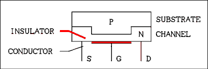
Figure 4.19 Metal Oxide Semiconductor FET.
For a verbal description click here.
The major difference between a JFET and a MOSFET is the gate or input resistance. For a JFET the typical input resistance is typically 1012 ohms while for a MOSFET the input resistance is typically 1016 ohms. MOSFETs are used in equipment which can measure currents in the picoampere range and below. Because of the high resistance of MOSFETs in a switching application, when they are off, they are really off. For this reason they find applications in very low power devices such as watches, calculators and lap-top computers.The substrate is the foundation on which the MOSFETs are constructed. In the case of discreet MOSFETs (as opposed to integrated circuits) the substrate may be brought out to a connecting lead of its own so the user may connect it as desired. The substrate is usually connected to the source although a P type substrate may be connected to the most negative point in a circuit. When MOSFETs appear in an integrated circuit, the substrate is the foundation on which the IC is constructed.
Enhancement Mode MOSFETs.
MOSFETs can be divided into two groups, depletion mode and enhancement mode. The group we have been talking about up until now are the depletion mode type, so called because they work by creating a depletion region in the channel. Depletion mode MOSFETs are "on" at zero gate voltage and a negative gate voltage will turn them "off".An enhancement mode MOSFET is "off" at zero gate voltage and a positive gate voltage (for an N channel) will turn it "on". The drawing of an enhancement mode MOSFET is shown in Figure 4.20.
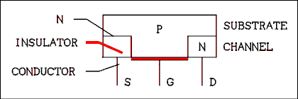
Figure 4.20 Enhancement Mode MOSFET.
For a verbal description click here.
In the case of an N channel MOSFET the substrate is P type semiconductor. Near the gate (between the source and drain) the substrate has been doped with both donor and acceptor impurities. The acceptors slightly outnumber the donors so the result is a lightly doped P type semiconductor. When the gate voltage is zero the P type semiconductor between the source and drain serves to block current between source and drain. When a positive voltage is placed on the gate, holes are repelled away from the gate. Once the holes are gone from this region, the donor impurities predominate and the material near the gate turns from P type to N type semiconductor. Current may now flow from source to drain.Enhancement mode MOSFETs are very rarely used as amplifiers. They most often appear in digital integrated circuits where they are used as switches.
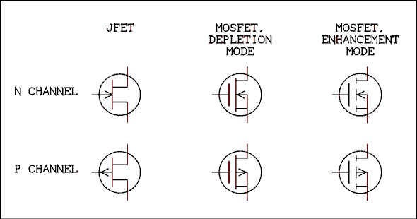
Figure 4.21 Schematic Symbols for Various Kinds of FETs.
For a verbal description click here.
Figure 4.21 shows schematic symbols for the various kinds of FETs. The FETs in the top row are N channel and the FETs in the bottom row are P channel. A good memory device is "the arrow always points toward the N type semiconductor". The bottom connection on each FET is the source. The connection on the left of each FET is the gate and the connection at the top is the drain. For MOSFETs the connection at center-right is the substrate. The substrate is shown connected internally to the source in these symbols. In some discreet MOSFETs the substrate is brought to a separate lead.For N channel FETs the drain is made more positive than the source. JFETs and depletion mode MOSFETs are fully on at zero gate potential. For operation as an amplifier, the gate is made more negative than the source. Enhancement mode MOSFETs are off at zero gate potential. For operation as an amplifier the gate is made more positive than the source.
For P channel FETs the drain is made more negative than the source. JFETs and depletion mode MOSFETs are fully on at zero gate potential. For operation as an amplifier, the gate is made more positive than the source. Enhancement mode MOSFETs are off at zero gate potential. For operation as an amplifier the gate is made more negative than the source.
Back to Fun with Transistors.
Back to Fun with Tubes.
Back to Table of Contents.
Back to top.
4.5 The FET as a Switch.
FETs are usually not used to turn lamps and relay coils on and off. They find two major applications, as logic switches and as analog (or signal) switches. We will cover the latter application first.The term analog switch may seem to be mutually contradictory. What is meant is to interrupt an analog signal to turn it off and on as desired or to select among several sources of signal. An example of the latter is the source selector in a stereo receiver. The switch allows the user to select among several program sources. Classically this has been accomplished by a mechanical switch. Newer designs which include remote control require electronic switching. This electronic switching may be accomplished using an FET.
Figure 4.22 shows an FET being used to switch an analog signal. The control voltage is +15 volts to turn the switch on and -15 volts to turn the switch off. The signal applied to the input must never exceed approximately plus or minus 10 volts. If the input signal comes too close to +15 volts, the switch can be turned off when it is supposed to be on. If the input signal comes too close to -15 volts, the switch can be turned on when it is supposed to be off.
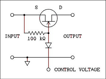
Figure 4.22 Analog Switch Using a JFET.
For a verbal description click here.
When the control voltage is positive, the diode is reverse biased, which disconnects the control voltage from the switched signal. The 100 k ohm resistor will cause the gate of the FET to be at the same potential as the source and the FET will be fully on. Signals applied to the input will appear at the output with little distortion or attenuation. When the control voltage is negative, the diode will be forward biased and the gate will be at approximately -15 volts. This will cause the FET to be turned off and very little or no signal from the input will be passed to the output. The 100 k ohm resistor will be connected from the -15 volt control signal to the signal source. In order for this circuit to work properly the signal source must have a low resistance for DC.Another type of analog switch is the CMOS (complementary MOS) device which comes in an integrated circuit. The IC operates from a single power supply (VDD) of up to 15 volts. The signal source must never go negative nor more positive than VDD. It is best for the AC signal source to be added to a DC of 1/2 VDD. If the signal part of the switch is forced outside of these limits by more than 0.7 volts the IC will, not may, but will be destroyed. The control voltage for this IC is zero to turn the switch off and VDD to turn the switch on.
A partial schematic diagram of the internal workings of this IC switch is shown in Figure 4.23. The triangle with a circle on its nose is an inverter. This is a switching device. If its input is zero, its output is VDD. If its input is VDD, its output is zero.
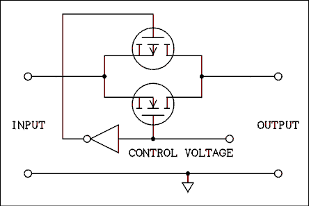
Figure 4.23 MOSFET Analog Switch.
For a verbal description click here.
The circuit is called complementary because it employs an N channel and a P channel MOSFET. When the control voltage is zero, the N channel FET has a gate voltage of zero and the P channel FET has a gate voltage of VDD. That turns both of them off. If the signal source is at a potential of VDD the P channel FET will still be off and the N channel FET will be negatively biased, which makes doubly certain that it will be off. If the signal source is at zero potential the N channel FET will still be off and the P channel FET will be positively biased, which makes doubly certain that it will be off. When the control input changes to VDD the N channel FET has a positive VDD on its gate while the P channel FET has zero potential on its gate. If the signal is at zero potential the N channel FET will be on but the P channel FET will be off. If the signal is at VDD the P channel FET will be on, but the N channel FET will be off. The two FETs are in parallel. So as long as one of them is on, the switch is on.The inverter is another example of how FETs are used as switches. Figure 4.24 shows the circuit of the inverter which was shown as a triangle in the circuit of Figure 4.23. When the input signal is at zero volts Q1 is biased fully on and Q2 is fully off. Thus the output is held to VDD. The output is high for a low input. If the input is VDD (high) Q1 is biased off (zero potential between gate and source) and Q2 is on. The output is low because it is held to ground by Q2. Whatever the state of the input, the output assumes the opposite state.

Figure 4.24 CMOS Inverter.
For a verbal description click here.
There are ICs which are known as invertors which contain six such circuits. Although they are not intended for use as analog devices, the input may be biased at 1/2 VDD and as such they make excellent amplifiers. (Which goes to show that if someone designs something, someone else will figure out a way to use it wrong and make it work.)Example 4.14.
A P channel depletion mode FET has -10 volts on its gate with respect to its source. Is it on or off?Solution:
A P channel depletion mode FET is on at zero potential and its drain current decreases as the gate is made positive. At +10 volts it would most likely be off but at -10 volts it is extremely on.Example 4.15.
An N channel enhancement mode MOSFET has a gate bias of zero volts. Is this FET on or off?Solution:
At zero volts between gate and source any enhancement mode MOSFET is off. The FET is off.Back to Fun with Transistors.
Back to Fun with Tubes.
Back to Table of Contents.
Back to top.
4.6 The FET as an Amplifier.
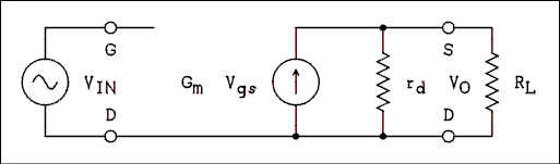
The FET has only two small-signal parameters, the drain resistance rd and the transfer conductance, called by contraction-loving electrical engineers transconductance Gm. The transconductance is defined as the AC drain current divided by the AC gate to source voltage with the drain to source voltage held constant.Gm = id / vgs with vds = 0 (4.37) The drain resistance is defined as the AC drain to source voltage divided by the AC drain current with the gate to source voltage held constant.
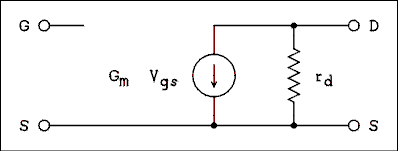
Figure 4.25 Small Signal Equivalent Circuit for an FET.
For a verbal description click here.
The Common Source Amplifier.
The common source equivalent circuit we will work from is shown in Figure 4.26. The input is an open circuit, as is the input of an FET. The output circuit consists of a current source which is dependent on the voltage between the gate and source. The drain resistance is in parallel with the current source. Any load is connected in parallel with the drain resistance.
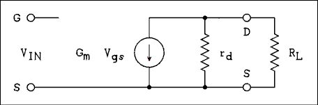
Figure 4.26 Equivalent Circuit of Common Source Amplifier.
For a verbal description click here.
The output voltage vo is the current source times the parallel combination of rd and RL.vo = -vin Gm rd RL / (rd + R/L) (4.19) Dividing through by vin and making the substitution AV = vo / vin we have,AV = -Gm rd RL / (rd + R/L) (4.20) where RL is the parallel combination of all resistors connected from the drain to AC ground.Amplifier Biasing.
A properly biased common source N channel JFET amplifier is shown in Figure 4.27. The battery VDD provides the positive bias for the drain and the battery VGG provides the negative bias for the gate. While this two-battery circuit will certainly work, it is not very practical.
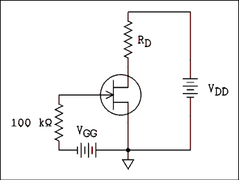
Figure 4.27 JFET Amplifier Using Battery Bias.
For a verbal description click here.
Figure 4.28a shows how the circuit may be rearranged without altering its operation. The negative connection point of VDD has been moved to the negative end of VGG, reducing VDD by the amount of VGG. This reduction is usually not significant enough to have any adverse effect. Notice that the polarity of VGG is the same as would be produced by the drain-source current flowing through a resistor in the source. Figure 4.28b shows the substitution of a resistor and a filter capacitor for the battery. The value of the source resistor sets the operating point.
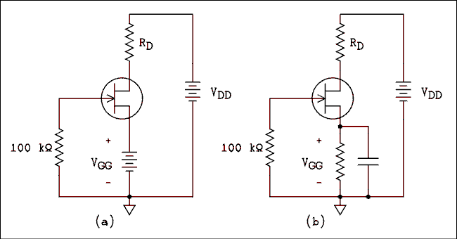
Figure 4.28 Converting Battery Biasing to Self Biasing.
For a verbal description click here.
Unlike for the BJT the operating point of the FET cannot be easily calculated. Some texts present a graphical solution which requires having a set of characteristic curves for the FET similar to those in Figure 4.18. Semiconductor manufacturers do not supply these curves for a very good reason. There is so much difference between FETs of the same type number that a set of curves would be useless. A semiconductor curve tracer interfaced to a computer and plotter could produce a set of curves for any individual FET and the graphic solution could be performed. Such a solution would be valid for only that one particular FET. Another FET would require another set of curves and a new graphical solution. We will not waste our time learning a useless procedure.The one and only advantage that FETs have over BJTs is their very high input resistance. In commercially designed equipment it is usual to see only one or two FETs among thirty or more BJTs. Even with such limited use, setting the operating point is a problem. There are two basic solutions. One is to use a trimming potentiometer (a screwdriver- adjusted variable resistor) as the source resistor as shown in Figure 4.29(a). Part of the calibration procedure includes setting the proper operating point of the FET amplifier. The other solution is to use the FET in conjunction with a BJT in an arrangement which will automatically set the operating point of the FET as shown in Figure 4.29(b).
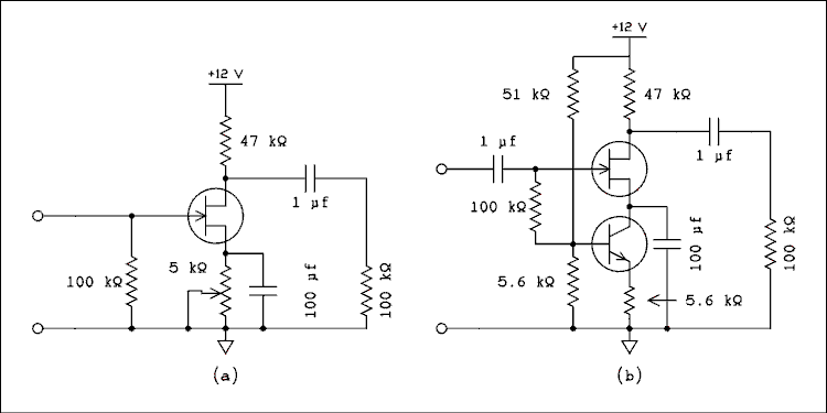
Figure 4.29 Practical JFET Amplifier.
For a verbal description click here.
Which one is used depends on who is to build the circuit. If the circuit is contained in a DIY article or a kit the reader or buyer is the one who constructs it. He does not receive a bill for his time at the end of each month so there is no cost associated with having him adjust the pot for the proper operating point.If the circuit is in a device which will be manufactured in the tens or hundreds of thousands and sold in retail stores the eventual owner cannot be held responsible for adjusting the pot. It must be done on the assembly line by a worker. It is an unavoidable fact that workers have to be paid. It is also a fact that workers do occasionally make errors. The expense of paying someone to adjust the pot will buy a lot of transistors. While the circuit at (b) is mor costly in terms of parts it is less expensive when fabrication costs are taken into account.
The (b) circuit works because the BJT sets the current through both transistors and holds it constant. The collector voltage, also the source voltage adjusts itself to what ever value is necessary to make the FET conduct the correct amount of current. The gate resistor is returned to the base to insure that the BJT will never be forced into saturation by the required gate to source voltage of the FET. The gate resistor in either circuit can easily go as high as 10 meg ohms if necessary.
Example 4.16.
In the circuit of Figure 4.29 the drain resistance of the FET is 130 k ohms and the transconductance is 600 micro mhos. What is the amplifier gain?Solution:
RL consists of the parallel combination of 47 k ohms and 100 k ohms, which is 32.0 k ohms. The gain of the amplifier isAV = -Gm rd RL / (rd + RL)
AV = -600 micro mhos x 130 k ohms x 32 k ohms / (130 k ohms + 32 k ohms) = -15.4
The Source-follower Amplifier.
Because the FET is used for its high input impedance, it is most often seen as a source-follower, as shown in Figure 4.30. The FET source-follower is characterized by very high input impedance, low output impedance and slightly less than unity gain.
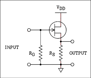
Figure 4.30 Source-follower Using N Channel JFET.
For a verbal descriptionclick here.
Figure 4.31 Equivalent Circuit of a Source-follower.
For a verbal description click here.
The equivalent circuit of a source-follower is shown in Figure 4.31. Summing the voltages around the outside loop we HaveVin = vgs + vo (4.21) In a source-follower the value of RL is usually much less than rd so we can neglect rd in the following equation. The output voltage is given byVo = vgs Gm RL (4.22) Solving equations 4.21 and 4.22 for vgs and setting them equal givesVin - vo = vo / (Gm RL) (4.23) Solving for vo / vin and remembering that AV is defined as vo / vin we have.AV = Gm RL / (Gm RL + 1) (4.24) As with the emitter-follower, the output impedance of the source-follower can be obtained by shorting the input, connecting a generator V across the output and determining the current I which flows. The output resistance is V/I. The equivalent circuit is shown in Figure 4.32.
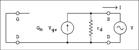
Figure 4.32 Finding Output Resistance of a Source-follower.
For a verbal description click here.
The current flowing through rd will be neglected. The current supplied by the generator is,I = Gm vgs (4.25) Because the input is short circuited vgs = V and so,RO = V / I = 1 / Gm. (4.26) The output resistance of a source-follower circuit is the parallel combination of the results of equation 4.26 and the resistor in the source of the FET. Note that unlike the emitter-follower the generator resistance has no effect on the output resistance.Example 4.17.
In the circuit of Figure 4.30 the value of RS is 1 k ohm and the transconductance of the FET is 3000 micro mhos. What are (a) the voltage gain and (b) the output resistance of the circuit?Solution:
(a) The gain is given byYou may be surprised by the low gain which is available from an FET source-follower. Designers seldom use a simple source-follower for just that reason. One very popular arrangement employs an N channel FET and a PNP BJT as shown in Figure 4.33. This circuit is often used as the input stage in oscilloscopes and AC voltmeters. This circuit is normally designed such that the collector current of the BJT is greater than the source current of the FET. This allows the BJT and the resistors to predominate in setting the operating point which eliminates the need for a trimming pot. Even so there is a DC offset between the input and output. The output may be anything from 1 to 4 volts more positive than the input. In DC coupled amplifiers such as those found in oscilloscopes this offset must be accounted for in some way to avoid adding it to the output.AV = Gm RL / (Gm RL + 1)
AV = 3000 micro mhos x 1 k ohm / (3000 micro mhos x 1 k ohm + 1) = 0.75
(b) The output resistance is
RO = 1 / Gm = 1 / (3000 micro mhos) = 333 ohms.
The output resistance is 333 ohms in parallel with 1 k ohm which is 250 ohms.
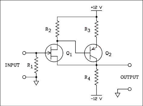
Figure 4.33 Unity Gain Impedance Buffer Using an FET.
For a verbal description click here.
Back to Fun with Transistors.
Back to Fun with Tubes.
Back to Table of Contents.
Back to top.
4.7 Differential Amplifier.
In the next chapter we will take up the study of operational amplifiers. A very important aspect of the op amp is its differential or difference input. A differential input consists of two input points with respect to ground. The circuit subtracts the two input signals. Thus the output of a differential amplifier isVO = AV (V2 - V1) (4.37) where AV is the voltage gain of the amplifier, V1 is the signal applied to the noninverting input and V2 is the signal applied to the inverting input.
The noninverting input is so named because an AC signal applied to this input is not inverted in phase. The inverting input is so named because an AC signal applied to this input is inverted in phase.

Figure 4.34 BJT Differential Amplifier.
For a verbal description click here.
Figure 4.34 shows a differential amplifier using BJTs. Q1 and Q2 work together to form the differential amplifier. Transistor Q3 along with R7, R8 and R9 form a constant current sink for the emitters of Q1 and Q2. The resistor network consisting of R7 and R8 keeps the voltage at the base of Q3 very stable regardless of changes in the base current of Q3. A very stable base voltage means that the emitter current will also be very stable and the collector current will also be very stable. Q3 carries the sum of the emitter currents of Q1 and Q2. If the emitter current in Q1 changes by a certain amount I, the emitter current of Q2 must change by an amount equal in magnitude and opposite in sign -I. This helps to maintain equal amounts of gain for both inputs.Resistors R5 and R6 introduce emitter degeneration in Q1 and Q2, which lowers and further equalizes the gains. In an amplifier of this type emitter degeneration is not a bad thing. The gain is set by the ratio of R3 to R5 rather than the parameters of the transistors. It should be noted that R3 = R4 and R5 = R6. If maximum gain is desired resistors R5 and R6 may be replaced by pieces of wire but Q1 and Q2 must be very closely matched (have identical parameters) if the gains from the two inputs are to be equal in magnitude.
The output may be taken in either one of two ways. Output 1 is taken between the collectors of Q1 and Q2 as shown. This is a differential or as it is sometimes called a push-pull output. It is suitable for driving another differential amplifier or a balanced transmission line. Some oscilloscopes employ differential amplifiers from beginning to end. The deflection plates of a CRT must be driven from a differential output for best performance.
Output 2 is taken between the collector of Q1 and ground. The input marked with a - sign is the inverting input. A positive-going signal applied to the base of Q1 will cause its collector current to increase. That increase will cause a larger voltage drop across R3 which will cause the voltage at the collector of Q1 to decrease. The input marked with a + sign is the noninverting input. A positive- going signal applied to the base of Q2 will cause the collector current of Q2 to increase. That increase in collector current of Q2 must be mirrored by a decrease in the collector current of Q1. A decrease in the collector current of Q1 will cause the drop across R3 to decrease. The decreased voltage drop across R3 will increase the voltage at the collector of Q1. In case you forgot, we started with an increase in the input voltage which shows that the input marked with a + sign is the noninverting input.

Figure 4.35 FET Differential Amplifier.
For a verbal description click here.
Figure 4.35 shows a differential amplifier employing FETs instead of BJTs. You will note that Q3, R7, R8 and R9 have been replaced by a symbol which you may have never seen before. This is the symbol for a constant current sink. It is commonly used when showing internal schematic diagrams of integrated circuits. The FET differential amplifier functions in exactly the same way as the BJT differential amplifier except its input impedance is much higher. Because FETs are even harder to match than BJTs, R5 and R6 are still necessary. Indeed they may be chosen to bring the gain down close to unity in order to balance the gains of the two transistors. FETs are used to obtain high input impedance. When large amounts of gain are needed, BJTs will be found in the circuit. If both are needed in the same amplifier, you will find both FETs and BJTs in the circuit.Back to Fun with Transistors.
Back to Fun with Tubes.
Back to Table of Contents.
Back to top.
4.8 Problems.
- The collector current of a BJT begins in the emitter, flows through the base region and ends up in the collector region. (This current refers to charge carrier current, not conventional current.) What kind of charge carriers (minority or majority) make up the collector current when it is in the (a) emitter region, (b) the base region, and (c) the collector region?
- In a PNP transistor the base current (conventional current) flows out at the base terminal. Where does it flow in?
- In the circuit of Figure 4.3 the values are as follows: VCC = 28 volts, beta = 150, VINON = 5 volts, VINOFF = 0 and RB = 8.2 k ohms. (a) If the lamp current is 65 mA, will the lamp be turned fully on? (b) After a few years the lamp burns out and someone replaces it with a lamp which draws 100 mA. Will this new lamp be fully turned on by the BJT switch? What will be the lamp current?
- In the circuit of Figure 4.4 VINON = 10 volts and VINOFF = 2 volts. R1 = 3.3 k ohms and R2 = 820 ohms. All other circuit parameters are as shown in the figure. Is the switch on when the control signal is high and off when the control signal is low? Show detailed calculations for both off and on states.
- For the starting conditions of problem 4, all of the students involved with designing and building the circuit have graduated. The transistor burns out and the equipment must be repaired because someone is giving a paper next week. Someone finds an old germanium transistor in a drawer and in desperation installs it in the circuit. The replacement has a beta of 100 but VBE to turn it on is 0.15 volts. Is the switch on when the control signal is high and off when the control signal is low? Show detailed calculations for both off and on states.
- For the starting conditions of problem 4, all of the students involved with designing and building the circuit have graduated. The transistor burns out and the equipment must be repaired because someone is giving a paper next week. Someone finds an old transistor in a drawer and in desperation installs it in the circuit. The replacement transistor is a silicon unit but its beta is 25. Is the switch on when the control signal is high and off when the control signal is low? Show detailed calculations for both off and on states.
- A transistor has the following parameters, hie = 2.5 k ohms and hfe = 85. If RL = 3.3 k ohms what is the gain of the common emitter amplifier?

Figure 4.36 Common Emitter and Emitter-follower Amplifier.
For Q1, hie = 2 k ohms and hfe = beta = 120.
For Q2, hie 30 ohms and hfe = beta = 55.
For a verbal description click here.
- Calculate the value of the collector current of Q1 in the circuit of Figure 4.36. Do not use an equation which is any more complicated than necessary.
- Calculate the value of the collector current of Q2 in the circuit of Figure 4.36. Do not use an equation which is any more complicated than necessary.
- Calculate the voltage gain of the emitter-follower stage in Figure 4.36. Remember to take everything into account when determining RL.
- Calculate the voltage gain of the common emitter stage in Figure 4.36. Remember to take everything into account when determining RL.
- The input resistance of a common emitter amplifier is equal to hie. What is the input resistance of the circuit of Figure 4.36?
- In the circuit of Figure 4.36 if the 75 ohm load were removed, what would be the output resistance of the circuit?
- What must the gate voltage be of an enhancement mode N channel MOSFET to (a) turn it on and (b) turn it off?
- What must the gate voltage be of an enhancement mode P channel MOSFET to (a) turn it on and (b) turn it off?
- Is it possible to make the circuit of Figure 4.23 work with depletion mode MOSFETs? Why or why not?
- Is it possible to make the circuit of Figure 4.24 work with depletion mode MOSFETs? Why or why not?
- A common source FET amplifier has a load resistance of 1.5 k ohms. The FET has a Gm of 3600 micro mhos and an rd of 200 k ohms. What are (a) the input resistance, (b) the voltage gain and (c) the output resistance?
- An FET source-follower has a load resistor of 10 k ohms. The FET has a Gm of 2600 micro mhos and an rd of 200 k ohms. What are (a) the input resistance, (b) the voltage gain and (c) the output resistance including the 10 k ohm load resistor?
- In the circuit of Figure 4.34 the collector current of Q3 is 1 mA. If the collector current of Q1 is 0.340 mA, what is the collector current of Q2?
- In the circuit of Figure 4.35 if the drain current of Q1 increases by 50 microamps, what happens to the drain current of Q2?
- If the gain of a differential amplifier is 10, V1 = +1.0 volt and V2 = +1.0 volt, what is the output voltage?
- If the gain of a differential amplifier is 100, V1 = +1.00 volt and V2 = +1.01 volt, what is the output voltage? Be sure to give sign as well as magnitude.
- If the gain of a differential amplifier is 100, V1 = +1.01 volt and V2 = +1.00 volt, what is the output voltage? Be sure to give sign as well as magnitude.
- If the gain of a differential amplifier is 100, V1 = -1.00 volt and V2 = -1.01 volt, what is the output voltage? Be sure to give sign as well as magnitude.
- If the gain of a differential amplifier is 100, V1 = -1.01 volt and V2 = -1.00 volt, what is the output voltage? Be sure to give sign as well as magnitude.
Back to Fun with Transistors.
Back to Fun with Tubes.
Back to Table of Contents.
Back to top.
4.9 Answers to problems.
- Part a, majority. Part b, minority. Part c, majority.
- At the emitter.
- Part a, required base current = 0.433 mA, supplied base current = 0.536. Lamp is fully on. Part b, required base current = 0.667 mA. The lamp is not fully on. Lamp current = 80.4 mA.
- On state. Required IB = 0.793 mA. Supplied IB = 2.12 mA. Switch is on. Off state. VBE unloaded = 0.398 V. Switch is off.
- On state. Required IB = 0.793 mA. Supplied IB = 2.80 mA. Off state. VBE unloaded = 0.398 V. BE is forward biased. Supplied IB = 0.378 mA. The switch will be between the on and off states.
- On state. Required IB = 3.17 mA. Supplied IB = 2.12 mA. The switch is not fully on. Off state. Same as in problem 4.
- AV = 112.
- IC = 1.20 mA by equation 4.24.
- IC = 47.2 mA by equation 4.23.
- AV = 0.987.
- AV = 43.6. Hint: There are 4 components that have to be added in parallel to make up RL.
- Rin = 1.57 k ohms.
- RO = 16.4 ohms.
- (a) Positive, (b) 0.
- (a) Negative, (b) 0.
- No. In the "on" state all is fine but in the off state one of the FETs will always be on.
- No. Both FETs would be on, draw excessive current, and burn themselves out.
- 1012 ohms, (b) -5.36, (c) 1.49 k ohms.
- 1012 ohms, (b) 0.963, (c) 370 ohms.
- ICQ2 = 0.660 mA.
- The drain current of Q2 will decrease by 50 microamps.
- VO = 0 V.
- VO = + 1.00 V.
- VO = - 1.00 V.
- VO = - 1.00 V.
- VO = + 1.00 V.
Back to Fun with Transistors.
Back to Fun with Tubes.
Back to Table of Contents.
Back to top.