
Practical / Implementation
Hardware
Transmitter
The transmitter is divided into the following segments:
|
|
Extended Parallel Port |
|
|
555-Timer |
|
|
JK Flip Flop |
|
|
Multiplexer |
![]()
Figure 3 – Transmitter Schematic
The block diagram below illustrates the basic operation of the transmitter segment.

Figure 4 – Transmitter Basic Operation
Extended Parallel Port
When using the extended parallel port, a set of tasks and labels are assigned to each line. Even thought the EPP is bi-directional, for the purpose of this project, it was used as unidirectional.
Before starting any EPP cycles by reading and writing to the EPP Data and Address Ports, the port must be configured. In the idle state, an EPP port has its nAddress Strobe, nData Strobe, nWrite and nReset lines inactive, high. Some ports require this to be set up before starting any EPP Cycle. These lines are to manually initialized lines using the SPP Registers. This is done by writing XXXX0100 to the control port.
The Parallel Port can only transport 8 bits at a time, thus any 32 or 16 bit word written to the Parallel Port will be split into byte size blocks and sent via the Parallel Port's 8 data lines. The pins 2 to 9 are the data pins of the extended parallel port which are in the sequence D0 to D8.
The diagram below illustrates this:

Figure 5 – Data pins of Extended Parallel Port
The Control port is used to read the least significant nibble. The control port has open collector outputs, i.e. two possible states, high impedance and GND. If the inputs are connected directly to the port, a conflict will result if the input is high and the port is trying to pull it down. Therefore open collector inverters (buffers) are used use. The parallel port is connected to the multiplexer via a buffer. The pin connection and configuration is shown in the diagram below where the inputs are from the parallel port of the computer and the output being pin from the buffer is to the input of the multiplexer:

Figure 6 – EPP Pin out Connection
555-Timer
The purpose of the 555-timer is to generate a frequency (50% Duty Cycle square wave). An operational amplifier is used between the 555-timer and the JK Flip Flop. This is to ensure that there is only one voltage input to the JK Flip Flop, either a high or a low.
The output pin is connected to the input pin of the JK Flip Flop. The pin outs for the 555-timer connections is shown below:

Figure 7 – 555-Timer Pin Out
See 555-Timer Datasheet in the
Appendix
JK Flip Flop
The M74HC73 is a high speed CMOS DUAL J-K FLIP FLOP WITH CLEAR fabricated with silicon gate C2MOS technology. Depending on the logic level applied to J and K inputs, this device changes state on the negative going transition of clock input pulse (CK). The clear function is accomplished independently of the clock condition when the clear input (CLR) is taken low. All inputs are equipped with protection circuits against static discharge and transient excess voltage.
The input accepted by the JK Flip Flop from the 555-timer is one voltage. This is ensured by the use of an operational amplifier (741). Since the flip flop is set high this voltage is converted to give an output broken down into two frequencies. These frequencies are that which is used for each appliance. Following the JK flip flop is the multiplexer.
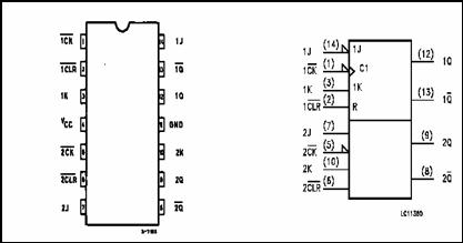
Figure 8 – JK Flip Flop Pin Out
See JK Flip Flop Datasheet in the Appendix.
Multiplexer
These data selectors/multiplexers contain inverters and drivers to supply full binary decoding data selection to the AND-OR gates. Separate output-control inputs are provided for each of the two 4-line sections.
The 3-state outputs can interface with and drive data lines of bus-organized systems. With all but one of the common outputs disabled (at a high-impedance state), the low impedance of the single enabled output will drive the bus line to a high or low logic level. Each output has its own strobe (G) inputs. The output is disabled when its strobe is high.
The multiplexer is connected to both the parallel port and the JK flip flop. It is connected to the parallel port via the pins G’, A & B. It is connected to the parallel port to obtain the signals being generated via the options. The multiplexer is connected to the counter to accept the four frequencies generated by the JK flip flop. With these two signals, the multiplexer knows which appliance is being chosen and chooses the particular frequency which corresponds to this option. Once the signal voltage has been determined, it is then transferred to the filter and handshaking circuits.
Below is an illustration of the multiplexers’ pin outs:

Figure 9 – Multiplexer SN54F253 Pin Out
See Multiplexer Datasheet in the Appendix
Filter
From the block diagram this is the coupling transformer. The filter circuit is used on both sides of the design i.e. on the transmitter side before the power line and on the receiver side after the power line. On the transmitter end, the filter circuit is used to convert the voltage signal being sent to a frequency greater than that of the power line. Using the filter circuit prevents any power surges and conflicts between the user’s signal generated and the power line signal. On the receiver end, the filter circuit is used to regenerate the frequency into a voltage to be transferred to the appliance.
Together with a filter circuit there is a handshaking circuit on both sides as well. This indicates when there is a high voltage spike, a wrong signal being sent or halt of signals. Handshaking is to prevent too fast of a flow of bytes from overrunning the system design i.e. when it can't process what it is receiving quickly enough and thus loses bytes and/or makes other serious errors. What handshaking does is halts the flow of signals until the power line is free and ready for some more signals.
The filter and handshaking circuits are both incorporated within the transmitter and receiver schematics. Note that there is a Schottky diode being used for the handshaking part of the circuit to limit the amount of current being passed through the circuit, hence increasing the benefit of reducing conflicts.
Power Supply
The power supply design, supplies power to all IC’s and the entire power line appliance controller design systems.
In the schematic below, the Voltage regulator circuit is to provide power to the parts of the circuits labeled 5V (see transmitter and receiver schematics), whilst the other power supply design is for all the IC’s where labeled +10V and -10V.

Figure 10 – Power Supply Schematic
Power Line
The uniqueness of this project is that the power line infrastructures already exist. However for simplicity and a better understanding of the of the actual power line this section is included.
From the street, the power company provides three cables to the home. One cable is called the neutral or common feed. The other two cables each carry approximately 110V of electricity. These cables are terminated at your home at a distribution box or breaker panel. Here, AC power is evenly distributed to multiple AC lines that run throughout the home. Each line is sent through a circuit breaker that prevents too much current from being drawn from any particular power line. Because there are two lines with 110V each from the street, there is usually enough available for the homeowner. If the homeowner uses a clothes dryer rated for 220 V, the two lines with 110 V are combined at the clothes dryer's receptacle. In some instances, there may be a third line of 110V run to the home.
AC power is viewed as a sine wave that cycles from a point called the zero crossing, where it rises to an equal distance above, then below, then back to the starting point, and 60 of these cycles in a one minute time frame is known as 60 Hz. The power company is required to regulate this value and keeps it constant. The cleanest point of the sine wave is the zero crossing. This is where you would look for and find a PLC signal. The PLC signal is a 5 V peak-to-peak (5 Vpp), 121 kHz message that is induced into the sine wave and rides along the AC wires with the AC power. The PLC signal has coded instructions that can only be heard by devices that are designed to listen for and react to these instructions. The devices that hear the signal are commonly referred to as smart modules.
Receiver
The receiver side repeats itself for each appliance. The only thing that changes is that the R's and C's have to be designed (chosen) for the corresponding frequency that controls that appliance. Normally the relay circuit routes signals coming over the power lines in the wall to input voltage circuit. The op-amp circuit is a buffer to prevent the high pass and low pass RC sections from loading and interfering with each other. The combination of R1-C1-buffer-RA-CA acts like a band pass filter that selects out and passes only the frequency that controls the appliance.
The receiver is divided in the following segment
|
|
Coupling Transformer |
|
|
Op-amp |
|
|
Tone Decoder |
|
|
Debouncer Circuit |
|
|
JK Flip Flop |

Figure 11 – Receiver Schematic
Basic Block Diagram of the Receiver end is illustrated
below, followed by the explanations.

Figure12 – Receiver Basic Operation
Operational Amplifier
This op-amp is used to boost the amplitude of the input signal, to facilitate the triggering of the device.
Tone Detector
The LMC567 is a low power general purpose LMCMOS tone decoder which is functionally similar to the industry standard LM567. It consists of a twice frequency voltage-controlled oscillator (VCO) and quadrature dividers which establish the reference signals for phase and amplitude detectors. The phase detector and VCO form a phase-locked loop (PLL) which locks to an input signal frequency which is within the control range of the VCO. When the PLL is locked and the input signal amplitude exceeds an internally pre-set threshold, a switch to ground is activated on the output pin. External components set up the oscillator to run at twice the input frequency and determine the phase and amplitude filter time constants.
The input from the filter circuit to the tone detector is via pin 3 which is its input pin and its output pin is pin 8 which goes to the D Flip Flop. So when that frequency and only that frequency signal is generated by transmitter side that signal is passed by only the receiver that has it's band pass filter corresponding to that frequency. That frequency signal is then detected by the tone decoder. This is then passed to the D Flip Flop.
See Figure 13 for Tone Detector Connection
See Figure 14 for Tone Detector Test Circuit
See Tone Detector Datasheet in Appendix
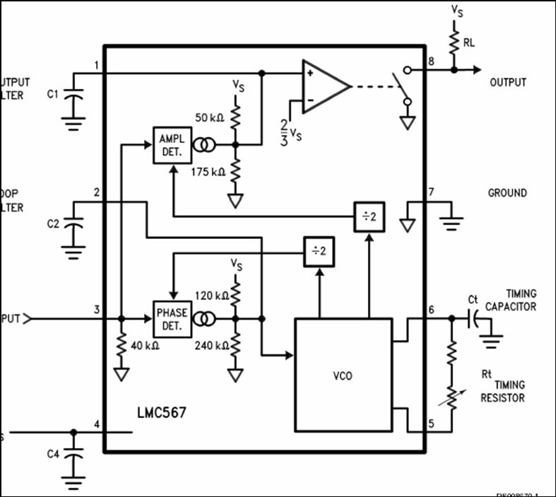
Figure 13 – Tone Detector Connection
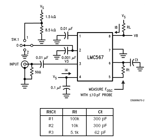
Figure 14 – Tone Decoder Test Circuit
Debouncer Circuit
A Schmitt Not gate was used here to provide two functions. First it would invert the low signal which will be sent to the D Flip Flop and second, acts as the debouncer circuit. This gives a delay on the IC’s output hence allowing the transition of the frequency input to settle. Therefore would provide a smooth triggering of the device.
D Flip Flop
Depending on the logic level applied to the D inputs, this device changes state on the negative going transition of clock input pulse (CK). The clear function is accomplished independently of the clock condition when the clear input (CLR) is taken low. All inputs are equipped with protection circuits against static discharge and transient excess voltage. The eight flip-flops will store the state of their individual D-inputs that meet the set-up and hold times requirements on the LOW-to-HIGH CP transition. When OE is LOW, the contents of the eight flip-flops are available at the outputs. When OE is HIGH, the outputs go to the high impedance off-state. Operation of the OE input does not affect the state of the flip-flops.
The D Flip Flop is used to determine the state of the appliance. That is, depending on the signal being sent, the flip flop toggles the relay and turns the appliance on/off. The same signal is used to turn the appliance on/off.

Figure 15 – D Flip Flop Pin Out
See D Flip Flop Datasheet in Appendix
