
The MJR7-Mk5 Mosfet Power Amplifier
TEST RESULTS.
BOARD LAYOUT.
PARTS LIST.
SETUP AND TESTING.
PHOTOS OF CONSTRUCTION.
DESIGN NOTES.
SUPPLY REJECTION.
MJR7 CONSTRUCTOR'S PAGE.
MJR7 Modifications
Latest updates:
(Updated Sept 2025) ON-Semi list the BC560C as obsolete. A possible substitute, the BC559CTA, is still 'active'. Alternatives need high gain at 5mA (500 plus) high Ft (200MHz plus) and low rbb' (160R or less). If high gain 200MHz PNP transistors are unobtainable 100MHz types could be substituted, but then the 1R5 input emitter resistor should be increased to 2R to preserve feedback phase margin.
The 2N3906 may be worth considering, fT minimum is 250MHz, but current gain could be less than 100. That will reduce loop gain a little and so increase distortion by a few dB, but stability is far more important. They're cheap enough, maybe buy 10 and select for highest current gain. The noise graphs suggest rbb' is less than 100R, so that's also ok.
The BC179C or BC179B are also options, they have fT minimum 200MHz, are allegedly 'low noise', and may have high enough gain. They are currently available (Sept 2025), made by CDIL. (Continental Device India Ltd.)(April 2017). In the circuit diagram I added a 5k6 resistor across the output of the 220R quiescent current adjustment preset. It is not entirely obvious what happens if the preset wiper becomes open-circuit, we don't want the quiescent current to then increase, and I am almost certain it will not, but for added security the 5k6 may be added. I have not altered the layout diagrams, it is easy enough to solder the resistor on the back of the board. I haven't added this to my own amplifiers. If the mosfets have zero drain to gate leakage there is no point, but I am not 100% certain about this.
(July 2012). I have added a link above to a page of 'design notes'. Most of that already exists somewhere, distributed around the various versions of the MJR7 on the old website. The Mk5 is almost certainly the final version, so a summary of the design philosophy is a useful addition.
(June 2012). The original 2SA1209 and 2SC2911 are becoming less easy to find. I have used the slightly better KSA1381 and KSC3503 in my own final version. I got these from Mouser in USA, they are actually KSC3503D and KSA1381E but the gain group is not critical. The 2SC2240BL are hard to find, a possible substitute is BC550C (ON-Semi), but the pin layout is different. 2SC2240 is E-C-B but the BC550 is C-B-E. The pnp transistor is now specified as a BC560C, made by ON Semiconductors if possible, some others have a lower specified fT. A high fT and current gain are the requirements. The mosfets could be any lateral type with similar case and specifications to the Renesas 2SK1058 and 2SJ162. The Renesas types have internal gate protection zeners, but possibly some of the alternative makes do not, so care is needed to protect the gates from static charge until connected to the board with the external zeners in place, e.g. keeping the gate and source connected together by a clip or metal foil. The external zeners are still a good idea even for the Renesas mosfets, the data sheet fails to mention the maximum current rating of the internal zeners. I checked with Profusion, and they tell me their Exicon mosfets do have 14V protection zeners with power rating around 1W, but not tested in production so not specified on the data sheet.
The compensation capacitor has now been reduced from 220p to 100p and its series resistor increased to 470R. To keep adequate stability margins with reactive loads two other changes then became necessary. The capacitor from input base to earth is increased from 330p to 470p (this is part of the compensation, not an input filter - the impedance at that point is just a few ohms because the feedback creates a 'virtual earth' - the other 470p is the only input filter), and also the resistor in parallel with the output inductor is reduced from 2R2 to 1R5 - this also reduces 'ringing' with a 2uF load.

I have included an anti-thump circuit, at the top left of the diagram, which consists of BAV20 diodes plus a resistor and capacitor. (Not my own idea, it is just a simplified version of a previously published circuit sent to me by a constructor of the earlier MJR6 which in its first version had a switch-on thump problem.) I reduced the capacitor across the LED biasing the KSA1381E current source to 1n to improve recovery from clipping, and this would make the switch-on pulse at the output worse, typically 8V. With 470uF in the anti-thump circuit the pulse is then not much over 1V, and slow, which makes just a small unobtrusive sound with my own speakers. ( Even this may still be a problem if directly driving mid-range or high frequency drivers in a bi-amp or tri-amp system. For this purpose the 4700uF output capacitor can be reduced, but then the 10uF in the feedback network and the 2u2 at the amplifier input must also be reduced in the same proportion. e.g. the values could be 470uF, 1uF and 0.22uF giving a -3dB low frequency gain around 60Hz.) The pulse can be reduced further by increasing the 470uF anti-thump capacitor, but there is then a longer delay before the amplifier reaches normal operation, it is about 15sec for each additional 470uF. At switch-on the capacitor starts to charge, which slows down the amplifier output capacitor charging pulse and so reduces the charging current through the speaker, but once fully charged the BAV20 diode connected to the KSA1381E is reverse biased, so there is no further effect on the circuit. The capacitor needs a voltage rating greater than the supply voltage used because in normal operation it is charged close to the full supply voltage.
The NPN input transistor Tr1 was originally a 2SC2547E, but this is becoming increasingly hard to find, and those I have bought recently include some obvious fakes far below the specified current gain range. More readily available types such as the 2SC2240BL can be used instead. The important specification is noise figure at 0.5mA collector current and 10k source impedance, and a figure under 1dB is good. If all else fails the BC550C should work well enough.
The PNP is shown as a BC560C, which I thought would have higher current gain than the original 2SA1085E, but testing a few samples I found little difference. The BC560C made by ON Semiconductors have a higher specified fT than some others, and this is useful because the pnp is the limiting factor in input stage bandwidth, which is relevant to overall feedback stability. The npn is effectively operating in common-base mode at very high frequencies as far as the local feedback loop is concerned, so it has a much higher bandwidth. For both input stage transistors avoid types with high base-spreading resistance rbb', this may add significant phase shift affecting loop stability.
Gain and Phase Shift
A Spice simulation gives the following result for closed-loop gain and phase shift. There is an almost perfect linear phase response from 1kHz to 20kHz, having the same effect in that frequency range as a constant time delay of 3.3usec, so having practically no effect on wave shapes. The -1dB frequency range is about 12Hz to 30kHz. The -0.5dB at 20Hz and 20kHz are unlikely to be noticeable, but simple additions to reduce these are suggested on the MJR7 Modifications page. At the end of that page I include another phase plot, but with a log scale for frequency instead of the linear scale used here. That more clearly shows what happens at low frequencies, but then a constant time delay is no longer a straight line, so I included a constant 3.3usec curve which shows that the deviation from constant delay is almost entirely a result of the input capacitor adding a phase advance at low frequencies, reaching +5 deg at 35Hz with a 4u7 capacitor.
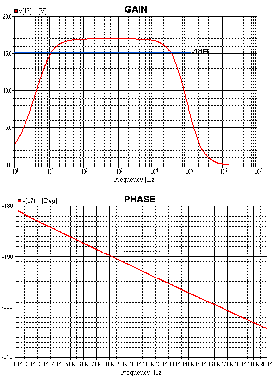
Also important are the feedback loop gain and phase shift, these determine how much the open-loop distortion, typically 2% at 10kHz, is reduced, and whether this has been achieved without sacrificing unconditional stability including with capacitive loads. The next plots don't include input stage effects, with a 200MHz fT PNP the unity gain frequency reduces to 4MHz with phase margin 37 deg. With a 2uF load the phase dips close to zero at 100kHz, but the loop gain is then above unity so still stable, and with shunt capacitance compensation the phase shift can be expected to fall near clipping before loop gain falls to unity, so instability is avoided. The test results page includes clipping with a 2uF load showing no signs of instability.


Board Design
The Mk5 includes two channels on one standard size board (6" x 4") with a single star earth included on the board.
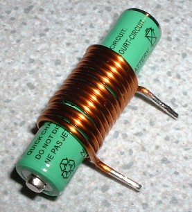
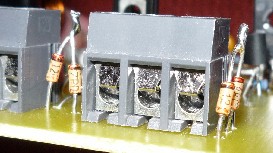
To avoid the mosfet mounting bracket used in earlier versions the mosfets are connected near the edge of the board so that they can be fixed directly to a heatsink. They could be soldered onto the board, but then there is some difficulty in ensuring they all line up correctly with the heatsink surface, and so the layout has been changed to allow the option of using terminal blocks as shown in the next photos. The blocks should be soldered in place before the 300R gate resistors so that these can be routed correctly to avoid obstructing the blocks. The inputs can also be taken to a terminal block if required.The coil, shown next, is air-cored, and is made using 18-gauge enamelled copper wire (1.2mm dia.) which can be made by winding it on a 1cm dia former, for example an AAA battery as shown in the photo. There are 13 turns, giving an overall length about 17mm. The other photo shows how the gate protection zeners are fitted. Only two holes are provided and the zeners have two ends soldered together off the board. The connected ends are the same polarity, in the photo the cathodes (indicated by a dark band) are connected, but it works just the same if anodes are connected together instead.
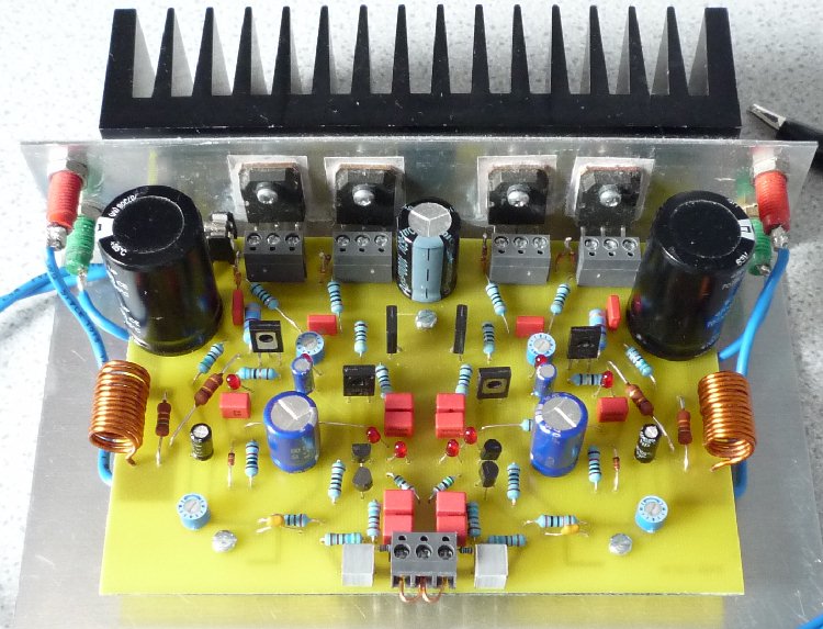
The next photo shows the final MJR7-Mk5.
Footnote: One problem with the inverting amplifier configuration is that with an open-circuit input it becomes a unity gain feedback amplifier, and the compensation needed to ensure stability can severely limit the performance. The 470p capacitor from input base to earth is the trick used to avoid this problem, and how this works is explained in Inverting Amplifier Feedback. The damping resistor across the output inductor is also important for stability, as explained in Output Inductor Damping. More details of the output network design are included in Output Network.
