The MJR7-Mk5 Design Notes
The Mk5 is almost certainly the final version of the MJR7, so a general explanation of the design philosophy is a useful conclusion.
The starting point was the MJR6, which was just an attempt to design the simplest possible class-B (or class-AB) amplifier circuit with adequately low distortion.
Using a capacitor coupled output makes it possible to avoid the entire differential input stage and apply the input direct to an only slightly more complex than usual voltage amplifier stage (VAS) using a complementary feedback pair plus cascode. Using lateral mosfets in the output stage these are driven direct from the VAS in the MJR6. Adding an emitter-follower stage for the MJR7 significantly reduced open-loop distortion caused by the non-linear mosfet input impedances.The circuit idea is not really new, in fact a very similar arrangement with inverting amplifier, output capacitor included inside the overall feedback, and a single voltage amplifier stage, was one of the first 'transformerless' solid state designs, published in 1956 by H.C.Lin. That used germanium transistors, and apparently the quiescent current stability was rather poor. Note that the original article showed this amplifier driven from a pre-amp, the output impedance of which determines the power amplifier gain. The circuit at the link given is therefore incomplete, and should have a series input resistor about 2k to define the gain if driven from a low impedance source.
Most modern amplifier designs use direct-coupled outputs, but the only unique achievement of direct-coupling is the ability to drive DC into the speaker, which we then need to prevent with speaker protection circuits. The only real problems with a capacitor coupled output are switch-on thumps as the capacitor charges through the speaker, some low level of capacitor distortion, and reduced low frequency damping factor. I included an anti-thump circuit, at the top left of the diagram, which consists of two BAV20 diodes plus a resistor and capacitor. This reduces the switch-on pulse to about 1V, which makes just a small unobtrusive sound with my own speakers, and there is no noticeable sound when switching off. There may of course be thumps or clicks from the signal sources if they are switched on or off while the amplifier is operational.
Including the output capacitor inside the global feedback loop reduces its distortion and also its effect on damping factor. The damping factor was specified for the Mk3 and that section is repeated here. The measured value of 1500 at 20Hz is better than for many direct-coupled examples.
DAMPING FACTOR:
This is included to demonstrate that the output capacitor effect is not only eliminated by the feedback loop, but the output resistance even becomes slightly negative around 10Hz. The damping factor is an almost entirely unimportant specification, the resistance of the speaker voice coil in series with the amplifier output impedance limits the level of speaker damping possible, so provided the damping factor is more than about 20 further increase makes practically no difference.
The values measured for an 8ohm load are:
380 at 1kHz
820 at 30Hz
1500 at 20Hz
Negative resistance -0.01ohm at 15Hz, -0.06ohm at 10Hz.
The damping factor at 20kHz was not measured at that time, but can be calculated as around 110, including the effect of the 0.4uH output inductor.
That negative output resistance is not likely to be a problem, possibly shorting the output could cause oscillation at around 10Hz, but all that would do is blow the supply line fuse, which would happen anyway if there is an audio input signal. In practice the negative resistance will cancel some of the resistance of the speaker cable, and in normal use it is of no importance.
SPEAKER PROTECTION:
The capacitor coupled output not only simplifies the circuit, it also protects the speaker under fault conditions. This can be done using other methods, but using an output capacitor for speaker protection gives more rapid effect than some methods using relays and other similar techniques. If fault conditions cause the output to short to the 60V positive supply rail then for a 4700uF capacitor feeding an 8R load the output pulse will start at 30V, but immediately start to fall, reaching 11V after 38msec. Using direct coupling together with a circuit to detect such an output and activate a relay to protect the speaker, a sufficient delay is needed to be certain the output is caused by a fault rather than high level bass. Add a few more msec for the relay to operate and the delay could be longer than the capacitor protection takes. The full supply voltage could be applied to the speaker during this time rather than a rapidly reducing voltage, so the probability of speaker damage may be significantly greater. Hopefully most speakers will survive such treatment, but some electronic music may have high level bass lower than 20Hz, so it is difficult to be sure how much delay is needed for all possible applications. There are alternative methods of detecting fault conditions, for example comparing input and output signals to determine any error, then far more rapid activation of the relay is possible, but then other sources of output error such as clipping could also activate the relay unless some clever circuit is devised to avoid this, or signal limiting is added prior to the amplifier input. The relay operating time delay resulting from its coil inductance can be reduced, for example by driving the coil from a much higher than specified voltage, but with a series resistor sufficient to prevent excessive dissipation.
INPUT STAGE DISTORTION:
Having combined the input and driver stages as a complementary feedback pair plus cascode we have an inverting configuration with 'virtual earth' input, and therefore no common-mode voltage to add distortion. Although I did an analysis to compare a number of simple input stages I made the point that once we have chosen to follow a high global feedback path the input stage becomes relatively unimportant. With open-loop gain 200,000 at 5kHz we find that for 20V at the output the input to the input stage is only 100uV. At this level even the worst of the input stages analysed, a single undegenerated bipolar transistor, has mostly second harmonic distortion at 0.1%. With 80dB loop gain this source of distortion is then reduced to 0.00001%.
Other forms of distortion such as TID and PIM are usually associated with input stage nonlinearity, and here also it is far easier to achieve adequate input stage linearity if it only has to handle 100uV.
The cascode stage is also essential for minimising input stage distortion. If we used either a single npn transistor or just the complementary feedback pair, then the whole output signal swing, up to 40V pk-pk, would appear at the input transistor collector. (Actually it would be greater than the amplifier output voltage swing because the output stage has a gain less than unity). I wrote a page about common-mode distortion which is relevant, even though there is no common-mode input to the MJR7 circuit. The point is that a large collector to base ac signal voltage will still cause 'Early Effect' distortion. The collector to base voltage modulates the depletion width of the base-collector junction, and this modulates the junction capacitance, the transistor current gain, and also the base-emitter voltage at a given collector current. Being in effect injected into the input, these sources of nonlinearity are not reduced by the global negative feedback, so it is important to minimise them by other means. The cascode stage keeps the input transistor ac collector signal very low, less than a millivolt, and reduces these effects to very low levels. The complementary feedback pair input stage has a moderately high output impedance because of the local feedback via the 1R5 resistor, and this helps increase the cascode stage output impedance.
GAIN BANDWIDTH PRODUCT:
This specification, often abreviated to GBW, is usually included as a single figure on op-amp data sheets, and is probably a more useful figure than open-loop gain, which is a function of frequency. With a -6dB/octave high frequency compensation the product of open-loop gain and frequency can be more or less constant over a wide frequency range, so just calculating or measuring gain at, say, 10kHz, and multiplying gain by frequency gives us a figure for the GBW. For the MJR7-Mk5 the gain at 10kHz is about the impedance of the 100pF compensation capacitor divided by the 1R5 used to set the value of gm for the input stage. The result is 10kHz x 160,000 / 1.5 which is about 1,000 MHz, or 1GHz.
Achieving closed-loop stability is not necessarily more of a problem with such a high GBW, instability can only occur at frequencies where the loop gain is close to unity, and all feedback amplifiers, with both high and low GBW, have a unity gain frequency and so are potentially unstable if the phase shift round the loop is not carefully controlled.
MORE DESIGN FEATURES:
The high frequency compensation capacitor and input stage current determine the slew rate limit, and with 100pF and 5mA we would expect around 50V / usec, which is the slew rate of a 20V peak sinewave at close to 400kHz. My measurements of peak slew rate for recorded music suggested that for most sources the amplifier only needs to be able to supply its full output swing up to 10kHz. The figure for the MJR7-Mk5 is therefore 40 times higher than this minimum requirement, giving an excellent safety margin. I only checked that full output is available up to 100kHz because that is the upper limit of my signal generator.
The method of applying high frequency compensation has some advantages. Using the 100pF from the cascode stage output to earth ensures that close to clipping the falling impedance at this point reduces the phase shift, and the stability margin improves. Stability is often a problem close to clipping in high feedback designs, so this shunt compensation method is a good choice.
If there is one 'magic' component which transforms this design into something more than ordinary, it is the 470p from the input transistor base to earth. The impedance at this point is just a few ohms because of the 'virtual earth' effect of the feedback, so the capacitor is not part of the input filter, it affects only the feedback loop, and together with the 10p in parallel with the global feedback resistor it provides a predictable attenuation of high frequencies round the feedback loop, and ensures that stabilisation is only required for an effective closed-loop gain of 47 at high frequencies, even though the audio frequency signal gain from input to output is only 18. The higher the closed-loop gain the more we can reduce the compensation capacitor. The 470p also avoids one serious problem of the inverting amplifier circuit, which is that with the input open-circuit it would otherwise become a unity gain amplifier, requiring heavy compensation to achieve stability, as explained in Inverting Amplifier Feedback..
The output inductor is not optional, the result of leaving this out can be an additional phase shift round the feedback loop as much as 100 degrees at high frequencies with a capacitive load. Then the amplifier will oscillate, or at best will be conditionally stable. Testing with clipping into reactive loads is unfortunately rare. In one of my failed designs there was perfect stability into any load with the usual square wave test, but clipping into a capacitive load triggered it into oscillation. The MJR7 has no problem with this test. I have seen some examples where clipping into even a resistive load provoked oscillation.
The damping resistor across the output inductor is important for stability, as explained in Output Inductor Damping. More details of the output network design are included in Output Network. (The inductor damping resistor was reduced in the final Mk5 version to maintain an adequate stability margin when the main compensation capacitor was reduced.) As explained there, the 100n plus 1R at the output are included to improve stability with small capacitive loads which could resonate with the output inductor close to the feedback loop unity gain frequency. An additional benefit of these components is that high frequency interference picked up by the speaker cables will be highly attenuated. The output inductor is of limited help with this because of the low value parallel damping resistor. Any interference still getting past the output network is fed back to the input stage via the 10p feedback capacitor, but is then attenuated further by the 470p from input base to earth, and so is reduced by another factor of 47. Using a high gain input stage could increase sensitivity to interference, but this is avoided by the effective filtering at both output and input.
There is yet another advantage of the capacitor coupled output, which is that only a single polarity power supply is needed. This actually becomes a disadvantage if we want higher power output because large value electrolytics rated anywhere above 63V are usually far more expensive. Using two 63V types in series, with equal parallel resistors to equalise the voltages is one way around this problem.
One advantage of the single supply is that it only needs a single fuse for protection, which avoids the problem with dual supplies that if a fuse fails in one supply the output could swing to the opposite supply rail, and careful design is needed to avoid such dangers. Failure of the single MJR7 fuse effectively removes all power from the amplifier.
The 2A-T fuse was originally specified for earlier versions with a single channel on each board, and in theory the single fuse for two channels on the Mk5 board should be rated for a higher current, but unless fuse failure at high sound levels is a frequent problem the 2A type can still be used. T-type anti surge fuses, according to some sources, can typically survive at 10 times their rated current for about 100 msec, and at 5 times the rated current for 1 sec, so a 2A supply line fuse is not the serious limit to output power that it may seem. With low impedance speakers driven at continuous high power however, it may be necessary to use a 3A-T fuse.
Regarding the need for protection of lateral mosfets, I have now found a diyAudio page I remembered seeing, called 'Lateral Mosfet Torture'. This describes attempts to destroy a lateral mosfet and the discovery of how difficult this can be. My use of a 2A-T supply line fuse has so far proved adequate, and I have never personally managed to destroy a mosfet even in higher power applications. If a lateral mosfet did fail my first suspicion would be that it was a fake, these are being sold in some parts of the world, but unfortunately the more reputable sources may be more expensive.Another advantage is that we only have a single supply rail with mains hum and other noises which we need to reject. The positive supply only connects to the output mosfets and to a current source which connects to a relatively low impedance point in the circuit, plus the bias chain. Supply rejection at 100Hz was measured as 99dB, which is very good.
Supply rejection is generally more important than supply design. Doubling the supply smoothing capacitor from 10,000uF to 20,000uF will only reduce supply line ripple by about 6dB, but supply rejection can vary by 100dB or more between different amplifier designs, so getting this wrong and trying to rectify the problem by an improved supply is not the best idea. Supply ripple does still matter a little if the amplifier is driven close to clipping because the ripple will reduce the output available before clipping.
There is one possible disadvantage to the output capacitor, which is that the maximum output level will fall at very low frequencies. My own speakers have impedance falling to 5.5 ohms at 10Hz or less, so with a 4700uF output capacitor the available peak output will fall by 3dB at about 6.2Hz. The 2u2 input capacitor however reduces the input signal by 3dB at 6.4Hz, so the required output would still be available. Thankfully recordings with high level components at 6Hz are either non-existent or at least extremely rare.
The MJR7 achieves excellent distortion figures using just a simple circuit with a single pair of lateral mosfets at 100mA quiescent current. Adding more parallel mosfets and running them at higher current would reduce distortion further, but unless far higher power output is needed this is an inefficient way to reduce distortion. A more efficient method is feedforward, and adding this to make the MJR9 reduced all measurable audio frequency distortion to under -120dB. With distortion already very low that seemed a step too far, with no serious point. It also needed accurate adjustment for best results using test equipment capable of detecting distortion down to around -130dB, so it was not an ideal DIY project. The MJR7 needs no selection or matching of components, and the adjustments need only a standard multi-meter.
Capacitor coupled outputs have become 'unfashionable', and this could equally apply to some of the other features. This was not entirely accidental, having read some doubtful claims concerning desirable amplifier design techniques I wanted to present a counter-example. There is virtually no circuit symmetry, only very little added local feedback via that 1R5 emitter resistor, and extreme levels of global negative feedback, regarded by some as the 'worst possible' sort. As for the shunt compensation technique, this is apparently 'in all respects sub-optimal' (see footnote 1). I had intended to reduce the open-loop -3dB frequency as low as possible, but failed there, it is probably high enough to qualify as above average. The use of a small polyester input capacitor, with allegedly audible problems of dielectric absorption, is of course optional, any other low leakage type could be used by those who believe in 'capacitor sound'. I remain entirely unconvinced on this issue, either theoretically or from my own tests or listening experiences, but did observe that using a capacitor with a large physical size could increase interference pickup by as much as 12dB over the whole audio frequency range, so capacitor choice can certainly have at least one real and easily measurable effect.
Another ignored 'principle' is that for a high slew-rate we need high value input stage degeneration resistors. For bipolar differential input stages this usually involves resistors around 100R in series with the emitters, or alternatively the use of jfets which already have lower gm without the resistors. My input stage has just 1R5, together with local feedback, giving a very high effective gm value, about 100 times higher than in some conventional designs, and yet the theoretical slew rate is a perfectly respectable 50V/usec.
Those typical degenerated input stages can only produce high slew rates for high level signals, in extreme cases they may need 1V or more differential input to achieve the specified slew rate. The MJR7 can produce its full slew rate with about 10mV at the input transistor base. Given that many signals have their maximum rate of change as they pass through zero a high slew rate at small signal levels may seem a good idea. This probably is of no importance for normal audio applications, but anyway I included an article about this 'problem', Slew Rate.
I should mention listening impressions, after all listening to music is the whole point, but I have too often been critical of 'subjectivist' evaluations, so it would be somewhat inappropriate to make any claims in this regard. I will simply observe that of all the people who have built my design and told me their listening experiences, all have been entirely complimentary.
DISADVANTAGES AND CRITICISMS:
Some disadvantages of the MJR7 circuit must be mentioned for completeness. The single supply has a problem compared to dual supply circuits, that it is more difficult to ensure symmetrical clipping. The 4k7 preset is to adjust the operating voltage of the mosfet sources to around half the supply voltage. It may be better to adjust instead for symmetrical clipping, but this requires the use of an oscilloscope, and even then will not be very precise, the setting will depend on the type of test signal used. I have sometimes used a 1kHz toneburst test signal, which affects the supply voltage less than a continuous sinewave and is closer to a typical music signal.
Also, the method of setting the operating voltage uses the base-emitter voltage of the input stage transistor as its reference, and this has a significant temperature coefficient, so adjustment will inevitably drift as the amplifier warms up, and so should be set up with the amplifier at its normal operating temperature. At one time I suggested a simple temperature compensation circuit to reduce this effect, but decided there was little if any point, the improvement in output level before clipping was unlikely to be more than a fraction of one dB, so unnoticeable, provided a reasonably well ventilated case is used to keep the internal temperature changes low.
Demanding symmetrical clipping is anyway questionable, even in a perfectly symmetrical circuit the clipping will only be symmetrical for a symmetrical signal such as a pure sinewave. Music signals are invariably asymmetrical, so one polarity will in practice always clip first as we turn up the volume. For optimum sound quality it is more important to avoid clipping entirely, which can be achieved by turning down the volume control, or using a more powerful amplifier or more sensitive speakers if a higher sound level is needed.
Another disadvantage is the noise level, which is not as low as we could achieve with a non-inverting series feedback circuit. With the inverting circuit there is a series input resistor which defines the input impedance, and if we choose this to be an acceptable value such as 10k this will add about 2uV input noise at 20deg.C and a 20kHz bandwidth. With a 1V input for full output this gives a 114dB signal to noise ratio, which is still very good, and unlikely to be a problem unless we want to use ultra-high sensitivity horn speakers. The complementary feedback pair at the input allows us to use a low noise input transistor operating at low collector voltage and at its optimum collector current for a good noise figure. The specified device has, according to its data sheet, a better than 0.5dB noise figure under the chosen operating conditions, and very low 1/f noise, so it adds very little to the input resistor noise.
A further problem is that the cascode stage and the driver stage transistor and current source reduce the available voltage swing, but again we are typically worrying about barely audible 1dB effects, and we can always use a slightly higher supply voltage if there is a requirement for a particular power output rating. Even the output stage bias adjustment circuit reduces the available output more than is really necessary, but it is done that way for a reason, which is to allow a 470R to be used in place of what was originally 100R connected from base to emitter of the emitter-follower stage, which contributed distortion because of the Early effect modulation of the base-emitter voltage. As I said in the original MJR6 article, squeezing out the maximum possible power rating was never a high priority, but I did try a 94V supply which achieved 79W into 7R5 with no obvious problems other than the driver stage transistors getting rather hot. Small heatsinks are probably a good idea for anything much higher than the recommended 60V supply. Use of the dual-die type lateral mosfets and closer to 100V supply should allow 100W output, but again the difference between 79W and 100W is a barely noticeable 1dB.
I have encountered one or two other criticisms, for example the input filtering is regarded by some as excessive. This may sometimes result from incorrect calculation, and possibly misunderstanding of the 2nd of the 470p capacitors, which is connected to the 'virtual earth' point where the impedance is just a few ohms and so it has little effect. That capacitor is an essential part of the high frequency compensation as explained here. The virtual earth has another important effect, which is that the 2nd 5k6 input resistor is effectively connected to earth for the purpose of calculating the filter response. The input filter is -3dB at about 120kHz, which I think is not unreasonably low. The 10p in parallel with the 200k global feedback resistor has a greater effect, giving the amplifier a further -3dB around 80kHz. The usual concern is the resulting phase error at audio frequencies, but a simulation shows that the MJR7 phase shift is almost perfectly linear from 1kHz to 20kHz, equivalent to a constant time delay of 3.3usec which can have practically no effect on wave shape and therefore no audible effect. The -3dB bandwidth of the whole amplifier is about 6Hz to 60kHz, which I believe is a reasonable choice.
To achieve the best possible performance we need to choose transistors with the best characteristics for this purpose. For example if we want low noise then some input transistors have lower noise figure than others. By all means use a BC109C at the input, but the noise should be lower with a 2SC2240BL. Similarly the voltage rating of the driver stage transistors appears to affect distortion, as does their collector-base capacitance, which is why I currently use 300V low capacitance types, KSC3503D and KSA1381E. The pnp input stage transistor has some effect on high frequency stability, and a high current gain combined with high fT helps with this. It is easy enough to change the circuit to make this less important, just increase the 1R5 degeneration resistor to 15R then almost any small signal pnp type can be used, but loop gain is then lower and distortion will be 10 times higher.
Footnote 1
The 'in all respects sub-optimal' quote is often attributed to Baxandall, for example on page 281 of 'Self On Audio' Second edition. Looking at the original 'Audio power amplifier design. Part 4', Wireless World, July 1978, p76, we find that this is a slight misquote, it should say 'sub-optimum', and it refers to shunt compensation applied 'across the first stage collector load' rather than the VAS output, though the same problems can apply in that case. In addition to describing the problem with this approach a solution is also given, which is to add a resistor in series with the capacitor, as in the MJR7 circuit. The point is also made (in Part 3) that shunt compensation is minimum phase, unlike the more common 'Miller compensation' which adds extra unwanted phase shift because of feedforward through the capacitor. It is sometimes said that this effect is only significant at very high frequencies far beyond the unity gain frequency of the feedback loop, provided the stage has high gm, but this is not necessarily true when the amplifier is close to clipping, where stability may already be a problem with some designs.Footnote 2
Whatever the advantages of a circuit design the performance can still be damaged by poor layout. My own board design is not necessarily the best possible, but the measurement results confirm that this layout has no serious problems. Some of those who built this circuit used their own board designs, and I can easily believe some of these will be better than my own, but I have no plans to build and measure different variations. There are well known requirements for good layout, one of which is to reduce the area of current loops, but it is also important to pay attention to the separation and relative orientation of different interacting loops. For example we can reduce the area of a current loop by using a double sided board with tracks on opposite sides, but the maximum magnetic field is then along the board, whereas for a single sided board with parallel tracks any loop will have greatest field perpendicular to the board where it may do less harm. Alternatively, a small board with closely spaced components may have smaller loops, which is good, but the loops are then closer together, which may not be so good.Footnote 3
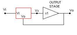
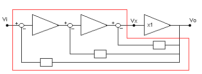
I was once asked whether I had thought of using alternative feedback arrangements, such as nested loops, error feedback, twin pole compensation, 'transitional Miller' compensation, and maybe others I forget. My answer then was 'no'. Not because I don't think they work, but because I think they have no inevitable advantage compared to simple single loop global feedback as used in my MJR7. This can be illustrated by a simple circuit shown next:This is the circuit diagram of all those feedback methods listed, and also the single loop, the only difference between any of them being the contents of the red box. Here, for example, is a multi-loop feedback version, showing the contents of the box.That box has two inputs Vi and Vo, and one output Vx which drives the output stage. Assuming we are concerned with class-B or class-AB amplifiers the primary purpose of the feedback is to reduce output stage distortion, and this is determined by the total feedback from the output of the output stage, round through the red box and back to the input of the output stage, so if we write Vx as a function of Vo that tells us everything about how far output stage distortion is reduced. Having chosen some function it makes no difference at all to the distortion reduction how we achieve that function. More to the point, none of those feedback techniques produce a unique function which could not be produced by any number of alternative circuits. If we want to maintain feedback level up to higher frequencies we can choose some second-order transfer function, but this can be achieved many different ways, all with identical effect. That assumes all such circuits are 'minimum phase' which in some practical examples is not so, but any minimum phase circuit with the required gain as a function of frequency is as good as any other. Any non-minimum phase circuit is less good.
There may be other reasons to choose a given circuit, for example the single global loop linearises the whole amplifier, not just some of the stages. It is also assumed that any internal feedback loops in the red box are adequately stable, and of course this is easier to achieve if there are no such loops, again the single global loop has an advantage. Applying the high frequency feedback round fewer stages may allow higher feedback loop gain in some cases, but by excluding the usual differential input stage to reduce the total number of stages, the MJR7 can still use high global loop gain without stability problems.