Figure 5.1 Noninverting Amplifier with Negative Feedback.
For a verbal description click here.
Chapter 5 Applying Feedback To Amplifier Circuits.
5.1 Some Preliminary Information.
5.2 The Negative Feedback Equation.
5.3 The Special Case of the Inverting Amplifier.
5.4 Frequency Response and Stability.
5.5 Gain Accuracy and Precision.
5.6 Other Benefits of Negative Feedback.
5.7 Some Practical Circuits.
5.8 Positive Feedback, Oscillators.
5.9 Problems.
5.10 Answers to Problems.
Chapter 5.
Applying Feedback To Amplifier Circuits.
If you have ever operated your school's sound system or have participated in a rock or country music band, you probably know the word "feedback". Feedback occurs when a fraction of the output signal is introduced into the input of an amplifier. The kind of feedback that sound system operators are familiar with is the squeal of positive feedback. This kind of feedback is undesirable but there are kinds of feedback which cause good things to happen. In this chapter we will study the desirable kinds of feedback.Back to Fun with Transistors.
Back to Fun with Tubes.
Back to Table of Contents.
Back to top.
5.1 Some Preliminary Information.
When feedback is introduced electronically its phase can be controlled. The signal which is fed back may reinforce or partially cancel the input signal. Feedback which reinforces the input signal is called positive feedback. Feedback which partially cancels the input signal is called negative feedback. We will begin our study of feedback with negative feedback.A major confusion factor has developed in teaching negative feedback because of a split among electrical engineers. One group, the audio engineers, sets out to derive the feedback equation by assuming a generalized amplifier. The equation they derive has a minus sign in the denominator. The other group, control systems engineers, assumes a net 180 degree phase shift in the feedback loop. In other words they assume that the feedback is always negative. The equation they derive has a plus sign in the denominator.
That would be bad enough by itself but the operational amplifiers (op amps) which are so useful have grown out of the control systems branch of electrical engineering. What this means to a teacher teaching a survey course in electronics is that when teaching feedback applied to audio amplifiers the equation with the minus sign must be used and when teaching op amps the equation with the plus sign must be used. That has proven to be so confusing to students that there is doubt as to whether they ever learned anything about feedback. In this book we will define away the problem by adopting one convention and sticking to it. If you look up the subject of feedback in another textbook you may find more confusion than help.
Back to Fun with Transistors.
Back to Fun with Tubes.
Back to Table of Contents.
Back to top.
5.2 The Negative Feedback Equation.
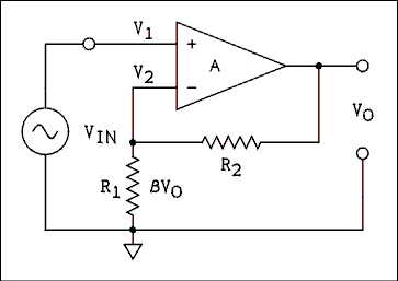
Figure 5.1 Noninverting Amplifier with Negative Feedback.
For a verbal description click here.
Figure 5.1 shows an amplifier with negative feedback applied. The amplifier is a differential amplifier which was discussed in the closing section of chapter 4. The signal generator is applied to the noninverting input of the amplifier. A fraction, beta, of the output signal is fed back to the inverting input. The difference between the two signals is amplified by the factor A and appears at the output.The output of a differential amplifier is given by equation 4.27 which is repeated here.
VO = A (V1 - V2) (5.1) As shown in Figure 5.1 V1 is the input signal and V2 is the fraction of the output signal beta VO. If we make these substitutions into equation 5.1 we haveVO = A (VIN - beta VO). (5.2) Solving this equation for VO / VIN we have the feedback equation.VO / Vin = A / (1 + A beta) (5.3) The term VO / VIN is called the closed loop gain and is given the symbol A', thus,A' = A / (1 + A beta) (5.4) where A' is the closed-loop gain, A is the open-loop gain and beta is the fraction of the output which is fed back to the input. This equation is to amplifiers as Ohm's law is to electric circuits. Memorize it.For the noninverting amplifier beta is given by
beta = R1 / (R1 + R2) (5.5) This beta is not to be confused with the BJT beta. They are not the same thing nor are they related in any way.Let us be sure we understand all of the terms associated with feedback. The open-loop gain (A) is the gain of the amplifier without any feedback circuits connected. The closed-loop gain (A') is the gain of the amplifier after the feedback has been connected. Beta, (it has no other name,) is that fraction of the output which is fed back to the input.
Example 5.1.
An amplifier has an open-loop gain of 250 and a beta of 0.02. What is its closed-loop gain?Solution:
The closed-loop gain is given byNote that we indicate this gain as a positive number. The circuit of Figure 5.1 is a noninverting amplifier which has no phase inversion. Such an amplifier has the signal applied to the noninverting input.A' = A / (1 + A beta) = 250 / (1 + 250 x 0.02) = 41.67.
Back to Fun with Transistors.
Back to Fun with Tubes.
Back to Table of Contents.
Back to top.
5.3 The Special Case of the Inverting Amplifier.
When the signal is applied to the inverting input, the circuit is called an inverting amplifier. An AC signal applied to the amplifier will be inverted by 180 degrees. When the value of the gain is stated it must be given as a negative quantity. The circuit of an inverting amplifier is shown in Figure 5.2. If you look in other texts similar to this one you are not likely to find the derivation of the gain of an inverting amplifier. The reason is that the equation which results from an exact derivation is slightly different from the one for a noninverting amplifier. Let us derive the equation and then we will discuss the difference.
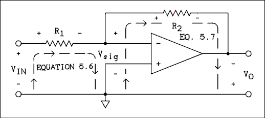
Figure 5.2 Inverting Amplifier with Equation Loops Indicated.
For a verbal description click here.
In Figure 5.2 the loops and polarity of all voltage drops are clearly marked. Consider these markings as a "snapshot" taken at the peak of the sine wave. Current flows from left to right through R1 and R2 thus causing the voltage drops to be as indicated on R1 and R2. Because of the nature of the amplifier the output voltage (VO) must have the opposite polarity as the input voltage (Vsig).If we write the loop equations around the loops labeled "equation 5.5" and "equation 5.6" we have
VIN = I R1 + Vsig (5.5) AndVsig = I R2 - VO. (5.6) The current I is the same in both resistors. The input resistance of the amplifier is very high and in actual practice the magnitude of Vsig is very small; hence any current flowing into the inverting input is very, very small. Therefore the currents in R1 and R2 are equal. Solving equations 5.5 and 5.6 for I and setting them equal gives(VIN - Vsig) / R1 = (VO + Vsig) / R2 (5.7) The nature of the amplifier requires that VO = A Vsig; therefore, Vsig = VO / A. Making this substitution into equation 5.7 gives.(VIN - VO / A ) / R1 = (VO + VO / A) / R2 (5.8) If we multiply equation 5.8 through by A, R1 and R2 we getR2 VIN A - R2 VO = R1 VO A + R1 VO. (5.9) After collecting VO terms, factoring out VO and performing some additional algebraic calisthenics we getVO / VIN = R2 A / (R2 + R1 A + R1) (5.10) Remembering that A' = VO / VIN and dividing numerator and denominator by R2 gives.A' = A / (1 + R1 / R2 A + R1 / R2) (5.11) For the inverting amplifier we will now define beta as follows.beta = R1 / R2 (5.12) If we substitute equation 5.12 into equation 5.11 and factor out beta we now have,A' = A / (1 + beta (A + 1)). (5.13) Compare equation 5.13 with equation 5.4 which is the gain for a noninverting amplifier.You are challenged to find equation 5.13 in any other text on this level. If all starting assumptions are correct and all of the algebra has been correctly done, the solution must be correct. Careful laboratory measurements using an amplifier with a low open-loop gain have shown that the equation does accurately predict the gain of an inverting amplifier. Equation 5.13 is the correct equation for the gain of an inverting amplifier.
A Difference Which Makes No Difference Is No Difference.
If the open-loop gain A is much greater than unity, equation 5.13 may be approximated by equation 5.4 with little detectable error. In actual practice open-loop gains are almost never less than 200 and may be as high as 107. Adding one to these large numbers will not make any practical difference. Unless the open-loop gain is less than 50, you need not bother with equation 5.13. Use equation 5.4.Example 5.2.
An inverting amplifier has an open-loop gain of -10. The values of the feedback resistors are R1 = R2 = 10 k ohms. (a) What gain is predicted by equation 5.4? (b) What gain is predicted by equation 5.13? (c) What is the percent error of equation 5.4?Solution:
For an inverting amplifier beta = R1 / R2 and if R1 = R2, beta = 1.00. (a) The gain predicted by equation 5.4 is.A' = A / (1 + A beta) = 10 / (1 + 10 x 1) = -0.9091.
(b) The gain predicted by equation 5.13 is.
A' = A / (1 + beta ( A + 1)) = 10 / (1 + 1 x 11) = -0.8333.
(c) The result of equation 5.13 is the standard; therefore, the percent error is + 9.10%
Example 5.3.
An inverting amplifier has an open-loop gain of -500. R1 = 10 k ohms and R2 = 200 k ohms. What is the closed-loop gain of the amplifier?Solution:<
The value of beta is beta = R1 / R2 = 10 k ohms / 200 k ohms = 0.0500. The open-loop gain is so much greater than unity that we can use equation 5.4.A' = A / (1 + A beta) = 500 / (1 + 500 x 0.05) = -19.23.
Example 5.4.
A noninverting amplifier has the same values as in example 5.3, A = 500, R1 = 10 k ohms and R2 = 200 k ohms. What is the closed-loop gain?Solution:
For a noninverting amplifier the value of beta isbeta = R1 / (R1 + R2) = 10 k ohms / (10 k ohms + 200 k ohms) = 0.047619
The closed-loop gain is.
A' = A / (1 + A beta) = 500 / (1 + 500 x 0.047619) = +20.15.
Back to Fun with Transistors.
Back to Fun with Tubes.
Back to Table of Contents.
Back to top.
5.4 Frequency Response and Stability.
Until now we have treated amplifiers as having a phase shift of 0 degrees (noninverting) or 180 degrees (inverting). As long as the frequency response is flat (gain does not change with frequency), these rules of phase shift apply. If the gain is rising or falling with frequency, there will be an extra phase shift which may cause trouble.The gain of an amplifier will change with frequency if there are RC networks inside the amplifier. These circuits may have been introduced intentionally or they may just be there. An example of an intentionally introduced RC circuit is the coupling capacitor between the collector of one BJT and the base of the next BJT. The resistance in the circuit and the capacitor form a high-pass filter. A semiconductor amplifier may not have any, or maybe one, of these circuits but a vacuum tube amplifier may have several.
Something never shown in schematic diagrams but always present in real circuits is stray capacitance. Remember that a capacitor consists of two conductors separated by an insulator. Any time there are two wires close together there is capacitance between them. That means that there are invisible capacitors connected from the collector of each transistor to ground and from the base of every transistor to ground. These capacitors combine with the Thevenin's resistance of the circuits to form low-pass filters. Each tiny low-pass filter causes the frequency response of the amplifier to roll off (gain decreases as frequency increases). Moreover, each transistor (BJT or FET) has its own built-in low-pass filter. Each device has its own frequency limits which are imposed by such things as collector-to-base capacitance and charge mobility within the semiconductor material.
The equations for phase shift (chapter 2) tell us that at the cutoff frequency the phase shift is 45 degrees. As the frequency gets higher than the cutoff frequency of a low- pass filter (or lower than the cutoff frequency of a high- pass filter) the phase shift quickly approaches 90 degrees. At the same time the gain is falling at a rate of a factor of 10 for each factor of 10 change in frequency.
Because the individual RC filters are isolated from one another by transistor stages, each one contributes to the total without affecting each other. If there are two RC filters with similar cutoff frequencies, the gain beyond cutoff will change by a factor of 100 for every factor of 10 change in frequency. The phase shift will approach 180 degrees. If there are three RC filters, the gain will change by a factor of 1000 for every factor of 10 change in frequency and the phase shift will approach 270 degrees. Gain change and phase shift go together like many other pairs of things you may have heard of. "You can't have one without the other." Thus, it is possible to know what the phase shift is even if you have no way of measuring it directly.
In the common operational amplifier, (op amp), the collector of the preceding transistor stage is directly coupled, not capacitively coupled, to the base of the next stage. This makes the frequency response go down to zero frequency which is DC. This is one of the few cases in electronics where it is possible to get something all the way to zero. Without any high pass filters in the amplifier the low pass filters that make the response roll off at the high frequencies are our only concern.
In some transistor amplifiers and all vacuum tube amplifiers there are high pass filters between each stage. These are capacitors in series with the signal path which are necessary to block the DC on the plate or collector of one stage from altering the bias on the grid or base of the following stage. The capacitors in conjunction with the resistors that connect to the control element of the amplifying device form high pass filters. These High-pass filters introduce phase shift and can cause low frequency oscillation if not designed properly.
The amount of phase shift depends upon the rate at which the gain is changing with frequency, which is determined by how many RC low-pass (or high-pass) circuits there are inside the amplifier. The rate of gain change is geometric. This means that a changing gain will be a straight line on a log- log graph. Figure 5.3 shows a log-log graph with various slopes (rates of change) plotted on it.
A rate of change of one decade decrease in gain for each decade increase in frequency is referred to as a slope of -1. If the gain decreases two decades for one decade increase in frequency, the slope is -2. If the gain should be increasing as frequency increases, the slope would be positive.
In the following discussion the phase shifts will be given with respect to the noninverting input. The phase shifts for the inverting input will be the algebraic sum of the stated phase shift and 180 degrees. If the slope of the frequency response is a negative 1, the phase shift will be -90 degrees. If the slope of the frequency response is -2, the phase shift will be -180 degrees. If the gain is falling with a slope of -2, the noninverting and the inverting inputs will be effectively interchanged. A connection which we thought would give negative feedback instead gives positive feedback. Positive feedback is the situation wherein the input signal is reinforced by the signal which is fed back instead of being partially canceled. When the input signal is reinforced, the output signal increases in amplitude. This causes the fed back signal to be increased which, in turn, causes the output signal to increase. This is a run- away condition and the input signal is no longer necessary; the amplifier is supplying its own input. An example is the earsplitting squeal of a sound system. This process is called oscillation and a device which oscillates is called an oscillator. When negative feedback becomes positive feedback we have an oscillator instead of an amplifier.
It would do no good to reverse the connections to the inverting and noninverting inputs. There would always be a part of the frequency spectrum where the gain is flat and there would be no extra phase shift. The circuit would oscillate because the feedback would be positive for those frequencies where the frequency response is flat.
In order to support oscillation two conditions must be met: 1) the net phase shift around the feedback loop must be zero and 2) the gain must be greater than unity. In order to prevent a feedback amplifier from oscillating, we must see to it that both conditions are not met at the same frequency. If at any given frequency only one of the two conditions is met, oscillation will not occur. The act of making internal changes to the amplifier so that both conditions will not be met at the same frequency is called amplifier compensation.
An amplifier which has not been compensated may well have a frequency response like that of the black line in Figure 5.3. A properly compensated amplifier could have a frequency response like the green line in the figure.
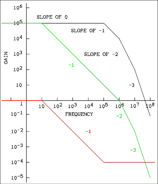
Figure 5.3 Bode Diagram Showing Compensation of an Amplifier.
For a verbal description click here.
It should be pointed out that the slope of real frequency response curves does not break suddenly from one slope to another. The curves make gradual and smooth transitions from one slope to the other as we saw in chapter two. What has been drawn in Figure 5.3 are the tangents to the curves. The tangents from the flat portion and the -1 slope portion intersect directly over the -3 dB point. That is why the -3 dB frequency is sometimes called the corner frequency.Examine the black curve in the above figure. It goes out flat to 100 kHz. Actually the frequency response is down 3 dB at 100 kHz but the Bode plot is drawn this way. At 100 kHz the plot breaks to a slope of -1. That means that one of the transistors started rolling off the frequency response. Another transistor in the amplifier begins to roll off at 1 MHz. This causes the Bode plot to break to a slope of -2. The plot falls by 40 dB, a factor of 100, between 1 and 10 MHz. At 10 MHz another transistor kicks in and the slope breaks to a slope of -3. After that the curve falls by 3 decades, 60 dB between 10 and 100 MHz.
What makes a feedback circuit oscillate is the loop gain not the gain of the amplifier. If this amplifier were to be used with a beta of 1/10000, it would not oscillate. 10000 is the value of gain where the slope breaks from -1 to -2. If a gain of 10000 is combined with a beta of 1/10000 the value of A beta is unity where the Bode plot breaks from -1 to -2 and the amplifier will be stable. Such a small value of beta would not be very useful but in audio amplifiers where the value of beta is fixed by the designer and does not change the Bode plot for A beta is used to compensate the amplifier instead of the plot of A alone.
On the other hand an op amp is frequently used with 100% feedback which is a beta of unity. To be useful an op amp must be compensated to unity gain. The way to convert the black curve in figure 5.3 into the green curve is to insert a passive circuit like that of figure 5.4 into the amplifier. This circuit produces the Bode plot of the red curve in the figure.
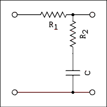
Figure 5.4 Schematic of Compensation Network.
For a verbal description click here.
The frequency where the red curve breaks from flat to a slope of -1, 10 Hz in this case, is given by,fA = 1 / (2 Pi C(R1 + R2)) (5.14.1) The frequency where the red curve breaks from -1 to 0, 100 kHz in this case, is given by,fB = 1 / (2 Pi C R2) (5.14.2) Notice that the short segment of -1 slope that is built into the amplifier is used by letting the network's plot flatten out just as the -1 slope of the amplifier is beginning.The amplifier whose frequency response is plotted in Figure 5.3 is DC coupled. Its frequency response goes flat all the way down to DC (zero frequency). An AC coupled amplifier might have a frequency response like that of Figure 5.5. In this example the upper end of the frequency response falls with a slope of -1 because it has already been compensated. The amplifier will not oscillate in this frequency range. At the low end, however, shown by the black line, the gain has a slope of +2 and is greater than unity. If feedback were applied to this amplifier, it would oscillate somewhere in the 0.3 to 10 hertz frequency range. Some internal changes will have to be made to this amplifier to make the positive portion of the gain slope become +1 from unity gain up to maximum.
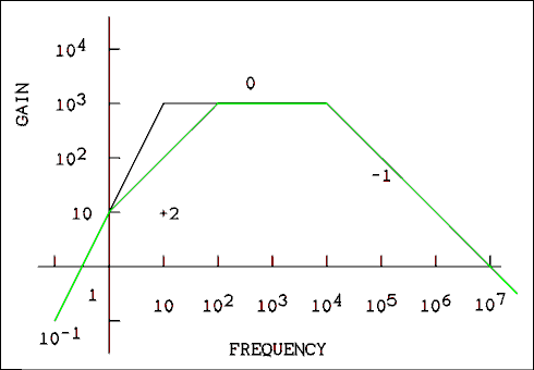
Figure 5.5 Bode Diagram with Low Frequency Role Off.
For a verbal description click here.
The black line plot in figure 5.5 is of the amplifier in figure 5.6. Capacitors C1 and C5, if they were numbered, are outside of the feedback loop. C3 is the cathode bypass of the second amplifier and common practice is to set such capacitors so the corner frequency for the RC circuit is very much less than one Hz. Experience has shown that the cathode RC has little effect on the phase shift of the amplifier even if the corner frequency is about one Hz. The resistor values have been fudged so the corner frequencies will fall on decade marks on the Bode plot. These values are not necessarily realistic.The capacitor values have been set the way a real, but amateur, designer would set them given the resistor values shown. Both break points have been set at 10 Hz which seems to be the reasonable thing to do. However the slope of the plot is plus 2 and the designer will find to his sorrow and possibly amazement that the circuit oscillates at a very low frequency. This kind of oscillation is often known as motorboating because it reminded someone of the sound of an old fashioned inboard motorboat.

Figure 5.6 Vacuum Tube Amplifier With Feedback.
For a verbal description click here.
The value of beta is 1/10 so the amplifier does not have to be compensated to unity gain. A beta must be compensated to unity which means the gain needs only to be compensated to 10 as shown by the green line. To do this one of the break points must be moved down to 1 Hz and the other one up to 100 Hz.It would not be good to move the C4 corner frequency up to 100 Hz because the output would rise below 100 Hz. So that one will be moved down to 1 Hz and the C2 corner frequency will be moved up to 100 Hz. This will give the green curve in figure 5.5. To make this amplifier stable C2 would have to be decreased to 0.001 microfarads and C4 increased to 1.0 microfarads.
Gain at Any Frequency, and Unity Gain Bandwidth (Gain-bandwidth Product).
An amplifier which has been properly compensated will have its gain change by one decade for every decade change in frequency, for all values of A beta greater than unity. A compensated amplifier may have a very large gain at middle frequencies but its gain can become quite low at the extremes of frequency near the unity gain frequencies.Let us take as an example a properly compensated AC coupled amplifier whose Bode plot is shown in figure 5.7. Its lower unity gain frequency is 0.1 hertz and its upper unity gain frequency is 100 MHz. The tangents to the frequency response curves (often called the Bode plot) are shown in Figure 5.7. As you can see from the figure, the gain is 10 at 1 Hz and 10 MHz.
To calculate the closed-loop gain of a feedback amplifier at any frequency we must know the open-loop gain at that particular frequency. We will recycle equations 2.24.4 and 2.24.5 from chapter two. You don't have to go back to look at them unless you want to see how they were derived. Those equations have a maximum value of unity. To adapt them for use here they must be multiplied by the maximum gain of the amplifier AMax.
Where f is the frequency at which the gain is desired, A is the desired gain, fc1 is the lower cutoff or corner frequency, fc2 is the upper cutoff or corner frequency, and AMax is the maximum gain. For an AC coupled amplifier, one that roles off at both ends of the frequency spectrum, AMax is the maximum gain that the amplifier reaches at mid band. For a DC coupled amplifier such as an op amp the maximum gain and the DC gain are the same thing. As long as you don't interchange fc1 and fc2 you shouldn't have any trouble knowing which equation to use.The frequency at which to change from using 5.15.1 to 5.15.2 is at the center frequency. This may not be what you assume. You must use the geometric center frequency which is given by,
fcc = sqrt(fc1 fc2) (5.15.3) Where fcc is the center frequency and fc1 and fc2 are as defined above. If you are working with an AC coupled amplifier, or a band-pass amplifier, use equation 5.15.1 above fcc and equation 5.15.2 below fcc.In a device such as an audio amplifier the values of fc1 and fc2 usually are easy to measure. For op amps and some very high gain band pass amplifiers the values of fcx are likely to be very difficult to measure so the unity gain frequency is measured and stated in specifications. To calculate the corner frequency from the unity gain frequency we use the following equations.
fc1 = flu AMax positive slope (5.15.4) andfc2 = fhu / AMax negative slope (5.15.5) where flu is the lower unity gain frequency, fhu is the upper unity gain frequency, fc1 is the lower corner frequency, and fc2 is the upper corner frequency.
Example 5.5.
A DC coupled (op amp) amplifier has a DC gain of 100,000 and a gain-bandwidth product (unity gain frequency) of 3 MHz. What is its gain at (a) 100 kHz, (b) 20 kHz, (c) 1000 Hz and (d) 5 Hz?Solution:
The Bode diagram for this amplifier would be similar in appearance to the green curve in Figure 5.3 but the values would be different. There are no positive slopes in the diagram and so we apply equation 5.15.5 to find fc2.fc2 = fhu / AMax = 3 x 10⁶ / 105 = 30 Hz.
(a) Using equation 5.15.1 we have
A = 105 / sqrt((105 / 30)2 + 1) = 30
(b) A = 150
(c) A = 2,999
(d) A = 98,639.
Example 5.6.
An AC coupled amplifier has a lower unity gain frequency of 0.1 Hz and an upper unity gain frequency of 100 MHz. Its mid-band (maximum) gain is 1,000. What is its gain at (a) 5 Hz, (b) 20 Hz, (c) 1 kHz, (d) 20 kHz, (e) 200 kHz and (f) 4 MHz?Solution:
The Bode diagram for this amplifier is shown in Figure 5.7. Making a Bode diagram is a good way to avoid mistakes in problems of this kind.
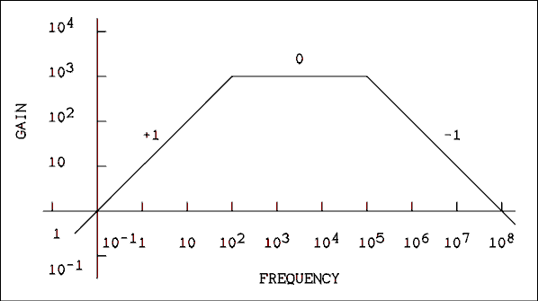
Figure 5.7 Bode Diagram for Example 5.6.
For a verbal description click here.
The first step is to find fc1 and fc2.
fc1 = flu AMax = 0.1 x 1000 = 100 Hz.
fc2 = fhu / AMax = 108 / 1000 = 105 Hz.
In order to decide which equation to use we must split the frequency response curve at the center of the flat portion. The center is the geometric mean of 100 Hz and 100,000 Hz. fcc is given by,
fcc = sqrt(100 x 100,000) = 3.16 kHz
(a), (b), and (c), are all below the center frequency and (d), (e), and (f), are all above it. Therefore we will use equation 5.15.2 for (a), (b), and (c), and 5.15.1 for (d), (e), and (f).
From equation 5.15.2 we have,
(a) A = 49.94,
(b) A = 196.1,
(c) A = 995.0
Now changing to equation 5.15.1,
(d) A = 980.6.
(e) A = 447.2,
(f) A = 24.99.
The Feedback Equation with Sloping Gains.
The examples above show how the magnitude of the amplifier gain varies with frequency. In order to make absolutely correct calculations of closed loop gain, taking phase shift into account, we would have to use the j operator. There is no mathematically rigorous way around it. You might suppose that we could use the Pythagorean theorem as we did in our study of RC circuits but the phase shift is not ninety degrees in the region around the corner frequency. The equation that produced the green line in figure 5.7.1 looks like this.

That equation seems to work but it trades off accuracy in one part of the frequency spectrum for inaccuracy in another. A graph will show what's going on.

Figure 5.7.1 Curves showing open-loop gain and
three calculations of closed-loop gain.
For a verbal description click here.
The graph shows frequency on a log scale versus dB. The numbers along the horizontal axis are the power to which you must raise 10, to obtain the frequency. The scale is from 0.1 to 100,000 Hz. Remember that ten to the 0 power is one. The red curve shows the open loop gain of a DC coupled amplifier with a DC gain of 10,000 and a unity gain bandwidth of 100 kHz. Notice that the gain is down by 3 dB at 10 Hz as it is supposed to be.The dark blue curve is the gain calculated from equation 5.4. Notice that it is down 6 dB at 100 Hz but it should be 3 dB down.
The green curve is calculated from the equation above. It is correct in this area of the spectrum, being 3 dB down at 100 Hz but the low frequency (DC) part of the curve is off by 1 dB, approximately 10%. As beta is made smaller this error gets worse. For a beta of 0.0001 the DC gain should be 5,000 which is 74 dB. The above equation, which has no number, gives 7,071 which is 77 dB. Such large errors in DC gain calculation cannot be tolerated so the no-number equation will be considered invalid and will not be used.
The equation which produced the light blue line is given below, along with its low frequency companion.
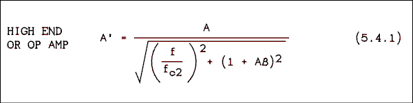
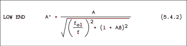
These equations were not so much derived as they were cloodged together to get the right answer. The light blue line behaves the way the real frequency response does. However, equations 5.4.1 and 5.4.2 will not be required in homework or test problems. They are presented for reference only.Example 5.7.
A beta value of .01 is applied to the amplifier of example 5.5. What is the closed-loop gain at frequencies of (a) 100 kHz, (b) 20 kHz, (c) 1 kHz and (d) 5 Hz?Solution:
(a) A' = A / (1 + A beta) = 30 / (1 + 30 x 0.01) = 23.08
(b) A' = 60.00
(c) A' = 96.77
(d) A' = 99.90
Back to Fun with Transistors.
Back to Fun with Tubes.
Back to Table of Contents.
Back to top.
5.5 Gain Accuracy and Precision.
Amplifiers without feedback have rather unpredictable gains. Transistor parameters vary with temperature and from one transistor to the next. Even if a one-of-a-kind amplifier were designed and constructed, its gain would change with temperature. If a transistor ever had to be replaced the gain would most likely change drastically.Amplifiers which are used in physics laboratories are involved with measurement of an electrical quantity. A changing gain in a measurement circuit will render the measurement useless. Negative feedback will stabilize the gain of an amplifier. How sensitive the closed-loop gain is to changes in open-loop gain can be determined through the use of calculus.
We will begin with the feedback equation
A' = A / (1 + A beta) (5.16) Using implicit differentiation to take the derivative of A' with respect to A we have,dA' = ((1 + A beta)dA - A beta dA) / (1 + A beta)2 (5.17) Splitting equation 5.17 into the difference of two quotients gives.dA' = (1 + A beta) dA / (1 + A beta)2 - A beta dA / (1 + A beta)2 (5.18) Now we will split the right-hand term into the product of two quotients and, at the same time, multiply everything to the right of the equal sign by 1 in the form of A / A and cancel (1 + A beta) in the first term. We now have,dA' = A / (1 + A beta) x dA / A - A / (1 + A beta) x A beta / (1 + A beta) x dA / A. (5.19) The right-hand side of equation 5.16 appears twice in equation 5.19. If we substitute 5.16 into 5.19 we now havedA' = A' x dA / A - A' x A beta / (1 + A beta) x dA / A (5.20) If we now divide through by A' and factor out the dA / A term we havedA' / A' = dA / A (1 - A beta / (1 + A beta)) (5.21) Simplifying the term inside the brackets gives,dA' / A' = dA / A x 1 / (1 + A beta) (5.22) This is where the EE book I used at university stopped. But The equation can be simplified still further. To shorten the notation let us say that E = dA / A and E' = dA' / A'. In this notation we can write,E' = E / (1 + A beta) (5.23) If we solve equations 5.23 and 5.16 for 1 / (1 + A beta) and set them equal we have.E' / E = A' / A (5.24) Because E' and E now appear as a ratio it doesn't matter if we express E' and E as fractional changes or percentage changes.This equation gives us one of the more important benefits of negative feedback, which is to stabilize the gain of an amplifier. Let us illustrate with an example.
Example 5.8.
An amplifier has an open-loop gain of 105 which may vary by as much as plus or minus 30%. The value of beta is 0.010. What is (a) the closed-loop gain, (b) how much is this gain in error referenced to 1 / beta, and (c) what is the percent variation in gain due to changes in open-loop gain?Solution:
(a) The closed loop gain isThis example shows that when the open-loop gain is very high, it has very little effect on the closed-loop gain. The closed-loop gain is set by beta which in turn is set by the values of two resistors. Resistors can be obtained as very high precision units.A' = 105 / (1 + 105 x 0.01) = 99.90
(b) Error referenced to 100 is -0.1%
(c) By equation 5.24
E' = E A' / A = 30 x 99.90 / 105 = 0.0300%.
It is often necessary to calculate how much open-loop gain is required or how much closed-loop gain can be obtained for a certain amount of gain error.
Example 5.9.
An amplifier has an open-loop gain of 5,000 which can vary by as much as 35 %. What is the maximum closed- loop gain available if the closed-loop gain variation is not to exceed 2.5 %?Solution:
Solving equation 5.24 for A' gives,A' = E' A / E = 2.5% x 5000 / 35% = 357.
Back to Fun with Transistors.
Back to Fun with Tubes.
Back to Table of Contents.
Back to top.
5.6 Other Benefits of Negative Feedback.
A fairly obvious question is "If negative feedback reduces the gain, why use it?" In the previous section we have seen that applying negative feedback to an amplifier will control its gain very accurately. That is not the only benefit of negative feedback. Almost any amplifier parameter you care to name is improved by applying negative feedback to it. Any amplifier designer will tell you that gain is the easiest of all parameters to obtain. The standard practice is to design an amplifier with much more gain than is needed and use negative feedback to trade the extra gain for improvement of all of the other parameters of the amplifier.Frequency Response.
Frequency response is improved by the application of negative feedback. The low frequency limits are moved lower and the high frequency limits are moved higher. For example look at the Bode diagram in Figure 5.8.

Figure 5.8 Bode Diagram of Closed and Open-loop Gains.
For a verbal description click here.
The frequency response of amplifiers is usually given in terms of the -3 dB points rather than the unity gain points. The open-loop gain of the amplifier whose Bode plot is given in Figure 5.8 has a frequency response of 1,000 to 10,000 hertz. Not exactly hi-fi is it? When negative feedback is applied to reduce the gain to 100, the frequency response becomes 10 Hz to 1 MHz. Quantitatively the improvement of frequency response is given by,f1' = f1 / (1 + A beta) (5.25) andf2' = f2 (1 + A beta) (5.26) Where f1 is the lower open-loop -3 dB frequency, f2 is the upper open-loop -3 dB frequency and the primes ' indicate the closed-loop equivalents.Distortion and Noise.
Distortion is defined as any alteration of the original signal by an electronic circuit. In audio circuits distortion is expressed as a percentage. When an absolutely pure sine wave is introduced at the input of an amplifier, the output consists of the original sine wave plus harmonics of the original sine wave. The total of the harmonics is expressed as a percentage of the original sine wave. This is often called the total harmonic distortion or THD of an amplifier. To a musician, distortion represents an alteration of the reproduced sound. To a physicist, distortion represents nonlinearity and errors in measurements. Distortion and nonlinearity are reduced by the addition of negative feedback to an amplifier as follows. Consider THD to be equivalent to nonlinearity.THD' = THD / (1 + A beta) (5.27) Noise is any varying voltage in a place where it is not wanted. It can be periodic as in the case of the 60 Hz line frequency which gets into everything. Noise can be aperiodic or random. Such noise is caused by the thermal agitation of charge carriers in conductors and semiconductors. The amount of noise N is affected by negative feedback as follows.N' = N / (1 + A beta) (5.28) It should be pointed out that because the signal is also reduced by the factor of 1 / (1 + Abeta) the signal-to-noise ratio is not improved by negative feedback but it isn't made any worse either. The fact that negative feedback is neutral when it comes to signal-to-noise ratio means that the other benefits of negative feedback can be realized without giving up anything really important.Input and Output Impedance.
The output impedance is lowered by the application of negative feedback by,ZO' = ZO / (1 + A beta) (5.29) In the case of a noninverting amplifier the input impedance is increased by an amount,ZIN' = ZIN (1 + A beta) (5.30) The input impedance which is affected is the input impedance of the transistor. Any fixed resistors which are outside of the feedback loop, such as base biasing resistors, will not be affected by the application of feedback.Back to Fun with Transistors.
Back to Fun with Tubes.
Back to Table of Contents.
Back to top.
5.7 Some Practical Circuits.
From time to time in this text, laboratory tested circuits will be presented. A circuit which actually works can illustrate a principle as well as one which looks as if it might work but probably will not. The latter kind of circuits are what are normally presented in electronics texts.It is not intended that you should memorize these circuits; they are given for possible future reference. Some day if you are in graduate school or a job and you need a circuit to accomplish some task, you may just find one here. Where practical, hints will be given on how changes may be made to the circuit to help you to adapt it to your particular situation.
The circuit of Figure 5.9 is a two-stage noninverting amplifier with feedback. The feedback is applied from the output, through the voltage divider consisting of R9 and the parallel combination of R10 and R4. For this circuit,
beta = R4 R10 / (R4 R10 + R9 (R4 + R10) (5.31) C2 is required because the tap on the voltage divider and the emitter of Q1 are at different DC voltage levels.The idea of applying a signal to the emitter of a transistor may seem strange. There is an amplifier configuration (not discussed) which is known as a common base or grounded base amplifier. In such a configuration the signal is applied at the emitter and taken out at the collector. Such an amplifier does not invert the input signal. Applying a positive-going signal to the emitter is the same as applying a negative-going signal to the base. Therefore, if a signal applied to the base is inverted, a signal applied to the emitter is not inverted.
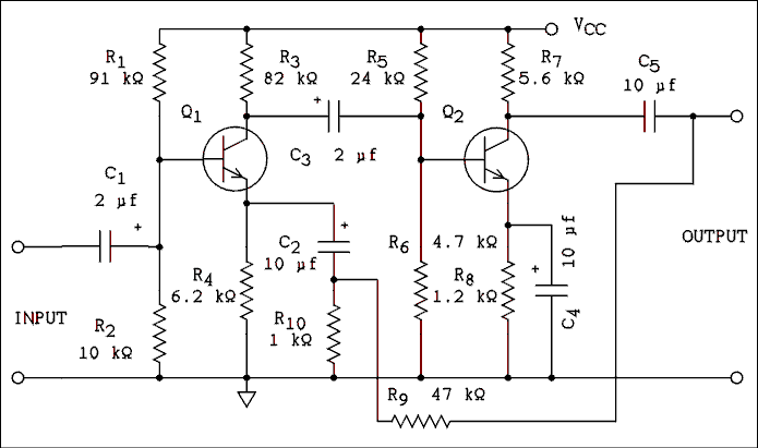
Figure 5.9 Laboratory Tested Circuit. Gain = 47, Frequency
Response is from 35 Hz to 600 kHz +0 -3 dB, Input Impedance
is 9 k ohms, Output Impedance is 700 ohms, VCC is 12 volts.
The gain may be altered by changing the value of R9.
The transistors are 2N3904.
For a verbal description click here.
The amplifier of Figure 5.9 has two BJT stages. The signal which is applied to the base of Q1 is inverted by that stage and applied to the base of Q2 where it is inverted again. Two inversions make a noninversion and, therefore, the base of Q1 is a noninverting input. A signal applied to the emitter of Q1 appears at its collector without being inverted. When this signal is passed through the Q2 stage it is inverted. Therefore, the emitter of Q1 is an inverting input. If negative feedback is to truly be negative, it must be applied to an inverting input.The circuit of Figure 5.9 contains a large number of resistors and capacitors because each transistor is individually biased. The circuit of Figure 5.10 eliminates the DC blocking capacitor between Q1 and Q2 and the biasing network in the base of Q2. A DC voltage exists at the collector of Q1 and a DC voltage is required at the base of Q2. The designer's trick is to make the two voltages equal and then eliminate the capacitor and biasing resistors. The base of Q2 gets its bias from the collector of Q1.
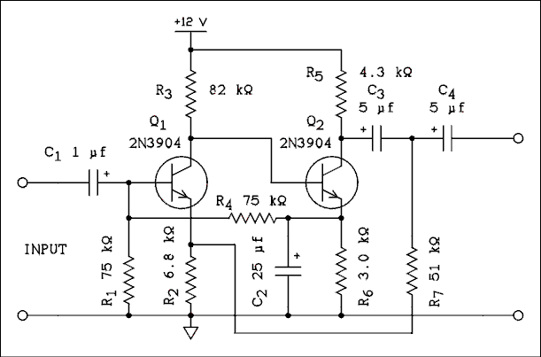
Figure 5.10 Laboratory Tested Circuit. Gain = 85,
frequency Response is from 4 Hz to 230 kHz +0 -3 dB,
input Impedance is 53 k ohms, output Impedance
is 580 ohms, Gain may be adjusted by changing R7.
For a verbal description click here.
This circuit is especially interesting because it has two feedback paths. One is from the emitter of Q2 to the base of Q1 and the other is from the collector of Q2 (the output) to the emitter of Q1. Capacitor C2 filters out the AC signal at the emitter of Q2 and so the feedback path from the emitter of Q2 to the base of Q1 is DC only. Because Q2 gets its base bias from the collector of Q1, any change in the operating point of Q1 will be amplified and passed to Q2. The DC feedback path provides operating point stability for both stages.If the emitter current of Q2 tries to increase, for whatever reason, the base bias on Q1 will be increased through the voltage divider consisting of R1 and R2. The increased bias on Q1 will cause its collector current to increase which pulls down its collector voltage. Since the base of Q2 is tied to the collector of Q1 the base bias on Q2 will be decreased, thus mostly canceling the increase in emitter current.
The AC gain is set by the AC feedback path which is from the output, through the voltage divider consisting of R7 and R4 to the emitter of Q1. In this case,
beta = R2 / (R2 + R7). (5.32) The value of R2 cannot be changed as this will upset the DC operating point of both transistors. R7 may be adjusted to set the gain to the desired value.Figure 5.11 shows another variation on the same theme. The advantage of this circuit over Figure 5.10 is that the output voltage swing can be almost equal to VCC. In the case of Figure 5.10 the base of Q2 is at the same potential as the collector of Q1, and so VCE + VRE of Q1 is not available for output voltage swing. The circuit of Figure 5.11 overcomes this by using a PNP and an NPN transistor. The emitter of Q2 is at VCC and the output voltage can almost swing from ground to VCC.
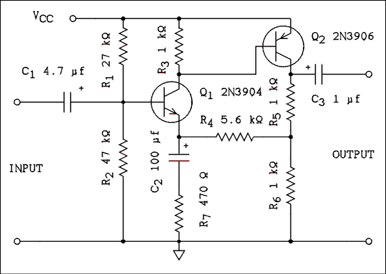
Figure 5.11 Laboratory Tested Circuit. Gain = 24,
Frequency Response is from 3 Hz to 1 MHz +0 -3 dB,
Input Impedance is 16.5 k ohms, Output Impedance is
332 ohms, VCC is 12 volts. The gain may be altered
by changing the value of R7.
For a verbal description click here.
The voltage divider consisting of R1 and R2 provides a constant bias for the base of Q1. For DC, 1/2 of the output is fed back to the emitter of Q1 for operating point stability. R4, R5 and R6 provide the DC feedback to the emitter of Q1. R7 and C2 combine to reduce the amount of AC feedback which will raise the AC gain of the amplifier. If R7 is shorted out, the amplifier will provide its full open- loop gain for AC. If R7 and C2 are removed from the circuit, the gain will be 2 for both AC and DC.beta = R6 R7 / ((R4 + R6 + R7)(R5 + R6) - R62) (5.33) If the circuit is to be used as a DC amplifier, capacitors C1 and C3 would have to be removed from the input and output. The circuit as given would introduce a DC offset to the signal. The resistor values probably could be adjusted to reduce the offset to near zero.Here is the circuit of a vacuum tube gain block. Gain blocks usually consist of two triodes with feedback from output plate to input triode cathode to diminish distortion to a very low level and tightly control the value of the gain. Here is a circuit I developed that will give a fairly wide range of gain at very low levels of distortion.

Figure 5.11.1 Vacuum Tube Gain Block.
For a verbal description click here.
This circuit has a lot of open loop gain which is traded off for low distortion. The gain may be changed by changing the cathode resistor, Rk, in the first triode. Changing this resistor has a very small effect on the operating point of either triode. The numbers are given in the table below.
| Cathode Resistor, Rk. | Gain. | Distortion. | Output Voltage. |
| 36 k ohms. | 6.67 | 0.035%. | 10 v. |
| 27 k ohms. | 8.47 | 0.04%. | 10 v. |
| 22 k ohms. | 10.1 | 0.045%. | 10 v. |
| 9.1 k ohms. | 21.7 | 0.045%. | 10 v. |
| 5.1 k ohms. | 33.6 | 0.060%. | 10 v. |
The value of beta for this circuit is given by,
Where Rk and Rf are as labeled in the schematic above.The feedback is DC coupled, not through a capacitor, from the plate of the second triode to the cathode of the first.
The 220 k ohm resistor makes up most of the load for the second triode which is where most of the distortion occurs. I don't recommend changing the value of Rf because it effects the operating point of the second triode. If this resistor is changed the cathode resistor in the second triode will have to be readjusted for minimum distortion.
Back to Fun with Transistors.
Back to Fun with Tubes.
Back to Table of Contents.
Back to top.
5.8 Positive Feedback, Oscillators.
It has been said that if a phase reversal slips into a negative feedback circuit, the amplifier will oscillate. There are circuits in which the feedback is deliberately made positive so as to generate an AC signal of known and constant frequency. Such circuits are known as oscillators.If we reverse the sign of the feedback the feedback equation becomes,
A' = A / (1 - A beta) (5.34) If A is less than 1 / beta the gain of the amplifier is increased over its open-loop value but it will still work as an amplifier. If A = 1 / beta the gain becomes infinite and the amplifier will provide its own input signal and will produce an output without any input. Mathematically if A is greater than 1 / beta the amplifier will oscillate and the amplitude of the oscillations will continue to build up and approach infinity. In the physical world amplifiers do not work this way. The amplitude will build up until the amplifier begins to saturate which has the effect of reducing the open-loop gain. The gain will be reduced until A = 1 / beta.Multivibrator.
The circuit of Figure 5.12 is at first glance two common emitter amplifiers, each one with its collector coupled to the other's base. Starting at one particular point and moving around the loop once, there are two 180 degree phase shifts which gives a total of 360 degrees, which is the same as a 0 degree phase shift. In actuality the transistors are acting as switches instead of amplifiers.
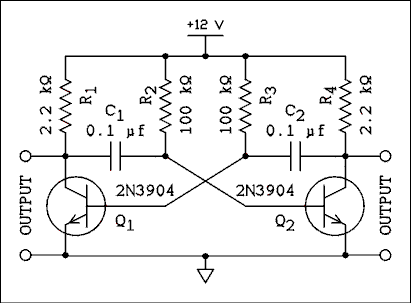
Figure 5.12 Laboratory Tested Circuit. Oscillation
frequency is 80 Hz, VCC may be as low as 1.5 v, Waveform
is approximately square, Amplitude = (VCC - 0.1) v P-P.
For a verbal description click here.
Let us start by assuming that Q1 is off and Q2 is on. The voltage at the collector of Q1 will be VCC and the voltage at the base will be negative because of remaining charge on C2. The voltage at the collector of Q2 will be approximately zero volts and the voltage at the base will be +0.6 volts. The charge on C1 will be equal to VCC - 0.6 v with the left-hand plate positive. C2 once had a charge of VCC - 0.6 v with the right-hand plate positive. C2 is now discharging through R3 causing the negative voltage at the base of Q1 to be headed in the direction of VCC. When the base voltage of Q1 reaches +0.6 volts, Q1 begins to conduct and its collector voltage begins to fall. This falling voltage is coupled through C1 to the base of Q2 which turns it off. When Q2 turns off, its collector voltage goes up and that change causes C2 to be charged through the base of Q1, turning it on very hard. Q1 is now on and Q2 is now off. C1 has a charge of VCC - 0.6 v with the left-hand plate positive. Because the left-hand end of C1 is clamped to ground by Q1 the base of Q2 is negative, insuring that it is off. C1 begins to discharge and the cycle keeps repeating with each transistor switching alternatively on and off.If R2 = R3 = R and C1 = C2 = C then the frequency of oscillation is given by,
f = 1 / (1.2 R C) (5.35) The frequency of oscillation is relatively insensitive to the power supply voltage.Circuits You May Find in Other Texts.
A good example of a circuit you may find in other electronics texts is the Wien bridge oscillator. This is a sine wave oscillator which, if properly designed, is capable of generating very pure sine waves. Back in the vacuum tube days this circuit used a tungsten lamp as a gain regulating element. The circuit was fairly simple and it worked quite well. Modern Wien bridge designs which employ a lamp do not work very well. A high-quality Wien bridge circuit is too complex to be presented in a text of this level. The simple circuits you may see in other texts are not laboratory tested and will likely not work. The writer refuses to waste space printing circuits which won't work.The Phase-shift Oscillator.
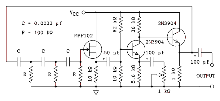
Figure 5.13 Laboratory Tested Circuit. This circuit operates
from 12 volts and with the given values will oscillate at
approximately 200 Hz. Its usable frequency range is from 5
Hz to 20 kHz. For best waveform use the pot to adjust the
output amplitude to 2.25 volts RMS. The waveform is a pretty
good sine wave.
For a verbal description click here.
The phase-shift oscillator works by using the phase- shift of an RC circuit. Oscillation requires a net phase- shift around the feedback path of zero degrees. The amplifier stage in Figure 5.13 provides a phase-shift of 180 degrees. Three cascaded high-pass filters are used to provide the additional 180 degrees of phase-shift. One RC filter will provide a maximum of 90 degrees of phase-shift and you might assume that two such circuits would be enough. The phase- shift of a high-pass filter reaches 90 degrees at infinitesimally low frequencies. At such low frequencies the attenuation is approaching infinity. When three filters are used each filter is required to provide a phase-shift of only 180 degrees / 3 = 60 degrees. Because the next filter loads the previous one each section does not provide exactly 60 degrees but the average is 60 degrees per section. Under these conditions the attenuation is finite and the circuit will work.There is only one frequency at which the total phase- shift is 180 degrees and it is given by,
f = 1 / (2 Pi sqrt(6) R C). (5.36) The attenuation of the circuit at this frequency is 1/29 and so the amplifier must have a gain of at least 29. The gain of the amplifier in Figure 5.13 may be set to 29 by means of the potentiometer. If the gain falls below 29 the circuit will stop oscillating. If the gain is higher than 29 the waveform will have a bit of distortion but the circuit will work reliably.Quartz Crystal Oscillator.
Quartz is a Piezoelectric material when properly cut. The meaning of Piezoelectric is that there is an interchange between applied electric field and mechanical deformation. If the cut piece of quartz crystal is mechanically deformed, an electric field will be developed across the quartz. If an electric field is applied to a quartz plate, the plate will be mechanically deformed.Because mechanical waves propagate through the quartz plate at a very high velocity, a thin plate of quartz will have a very high mechanical resonant frequency (roughly from 10 kHz to 100 MHz). The Piezoelectric effect allows this mechanical resonance to be transformed into an electrical resonance.
The quartz crystal behaves as if it were an LC resonant circuit. Crystals have two major advantages over LC circuits. They are 1) the quartz crystal is usually smaller than an LC circuit tuned to the same frequency and 2) the crystal has a much higher Q than an LC circuit tuned to the same frequency. The highest achievable Q values for an LC circuit are 250, although 100 is more typical. Crystal Q values range from 1,000 to 10,000. The only disadvantage of a quartz crystal is that its frequency cannot be adjusted once it leaves the factory.
When a quartz crystal is used as the frequency- determining element of an oscillator (as opposed to an LC circuit), the oscillator frequency is much more accurate and stable. The much higher Q of the crystal is what makes the oscillator frequency so much more stable.
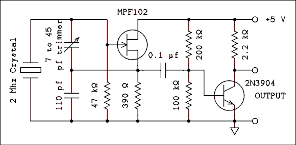
Figure 5.14 Laboratory Tested Circuit. This is a quartz
crystal oscillator with a frequency of 2 MHz and an
output suitable for driving one TTL logic load.
For a verbal description click here.
Figure 5.14 shows the diagram of a 2 MHz quartz crystal oscillator. The 7 to 45 pf trimmer capacitor may be used to adjust the frequency over a very small range, typically 0.05% of the crystal frequency. The JFET section is the oscillator circuit. This section could be constructed alone and the output taken from the source of the FET. The BJT portion operates as a switch and it is turned on and off by the AC signal from the oscillator portion. The entire circuit should work perfectly using a 1 MHz crystal. The oscillator section has been tested using a 10 MHz crystal but the BJT switch has not.If you apply what you know about switching circuits you will find that the BJT is neither fully on or fully off. That is desirable in this application because the AC signal from the oscillator will drive the switch alternately on and off. If the switch were set fully off, the AC signal from the oscillator might not have enough amplitude to turn it on.
Back to Fun with Transistors.
Back to Fun with Tubes.
Back to Table of Contents.
Back to top.
5.9 Problems.
- An amplifier has an open-loop gain of 300 and a beta of 0.01. What is its closed-loop gain?
- A noninverting amplifier has an open-loop gain of 8. R1 = R2 = 12 k ohms. What is the closed-loop gain of this amplifier?
- An inverting amplifier has an open-loop gain of 8. R1 = R2 = 12 k ohms. What is the closed-loop gain of this amplifier?
- A noninverting amplifier has an open-loop gain of 1,000. R1 = 10 k ohms and R2 = 40 k ohms. What is the closed-loop gain of this amplifier?
- An inverting amplifier has an open-loop gain of 1,000. R1 = 10 k ohms and R2 = 40 k ohms. What is the closed-loop gain of this amplifier?
- An amplifier which has a Bode plot similar to that of Figure 5.4 has a DC gain of 75,000 and a gain-bandwidth product of 1.5 MHz. What is its gain at frequencies of (a) 100 kHz, (b) 20 kHz, (c) 1 kHz, (d) 20 Hz, and (e) 5 Hz?
- If negative feedback is applied to the amplifier of problem 6 and the value of beta is 0.013333, what is the closed-loop gain at frequencies of (a) 100 kHz, (b) 20 kHz, (c) 1 kHz, (d) 20 Hz, and (e) 5 Hz?
- An amplifier which has a Bode plot similar to that of Figure 5.5 has a lower unity gain frequency of 0.5 Hz, an upper unity gain frequency of 10 MHz and a maximum gain of 300. What is its gain at frequencies of (a) 5 Hz, (b) 20 Hz, (c) 200 Hz, (d) 1 kHz, (e) 20 kHz (f) 50 kHz, and (g) 2 MHz?
- If negative feedback is applied to the amplifier of problem 8 and the value of beta is 0.025, what is the closed-loop gain at frequencies of (a) 5 Hz, (b) 20 Hz, (c) 200 Hz, (d) 1 kHz, (e) 20 kHz, (f) 50 kHz and (g) 2 MHz?
- An amplifier is required to have a gain stability of 0.5%. The open-loop amplifier has a gain stability of 20%. If the closed-loop gain is to be 200, what must be the minimum open-loop gain of the amplifier?
- An amplifier has a closed-loop gain of 1,000 and an open-loop gain of 100,000 plus or minus 50%. What is the closed- loop gain error?
- An amplifier has an open-loop gain of 300,000 plus or minus 40%. What is the maximum closed-loop gain available if the error in the closed-loop gain is not to exceed plus or minus 1%?
- What is the calculated value of beta of Figure 5.9?
- In Figure 5.9 if the open-loop gain is 280, what is the closed-loop gain?
- In Figure 5.12 if resistor values are as given, what must the values of C1 and C2 be to give an oscillation frequency of 60 Hz?
- In Figure 5.13 if all capacitors marked C are 0.001 uf, what must be the value of the resistors R to give an oscillation frequency of 440 Hz?
- In Figure 5.14 if there were no AC signal from the oscillator, what would be the value of VCE of the BJT? Assume beta = 100.
Back to Fun with Transistors.
Back to Fun with Tubes.
Back to Table of Contents.
Back to top.
5.10 Answers to Problems.
- 75.
- 1.6.
- -0.8.
- 4.975.
- -3.98.
- (a) 15.0, (b) 75.0, (c) 1500, (d) 53,033, (e) 72,761.
- (a) 12.50, (b) 37.50, (c) 71.43, (d) 74.89, (e) 74.92.
Note. These calculations are correct not just close.
If you didn't hit the numbers on the nose,
you must have done something wrong.
- fc1 = 150 Hz, fc2 = 33,333 Hz, fcc = 2,236 Hz.
(a) 9.994, (b) 39.65, (c) 240.0, (d) 296.7, (e) 257.2, (f) 166.4, (g) 4.999.- (a) 7.996, (b) 19.91, (c) 34.28, (d) 35.25, (e) 34.62, (f) 32.25, (g) 4.444.
- 8000.
- 0.5%.
- 7,500.
- 0.01799.
- 46.38.
- 0.13 microfarad.
- 148 k ohms.
- 1.48 volts.
Back to Fun with Transistors.
Back to Fun with Tubes.
Back to Table of Contents.
Back to top.