
Figure 8.4 AND Function Illustrated Using Switches.
For a verbal description click here.
| A | B | C | LAMP |
| 0 | 0 | 0 | 0 |
| 0 | 0 | 1 | 0 |
| 0 | 1 | 0 | 0 |
| 0 | 1 | 1 | 0 |
| 1 | 0 | 0 | 0 |
| 1 | 0 | 1 | 0 |
| 1 | 1 | 0 | 0 |
| 1 | 1 | 1 | 1 |
Figure 8.5 Truth Table for AND Function.
Chapter 8 Digital Circuits.
8.1 The Binary Number System.
8.2 Logic Functions and Gates.
8.3 Boolean Algebra.
8.4 Combinational Logic Circuits.
8.5 Flip-Flops and Counters.
8.6 Displaying the Count.
8.7 Multiplexed Displays.
8.8 Digital to Analog Converter.
8.9 Analog to Digital Converter.
8.10 The 555 Timer.
8.11 Problems.
8.12 Answers to Problems
Chapter 8
Digital Circuits.
Up to this point we have been dealing with analog signals. An analog signal is a voltage or current which carries information and can take on any value. For example the output of a thermocouple can be 31.56 uV or 103.97 uV or even 1.6358 mV. The point is that the only limit is our ability to measure the voltage. The voltage itself may have a value of 1.63582419574239658395723656793445642467543 mV for all we know. Analog data is quantized (if at all) only by the measurement technique. The data itself may take on any value.Digital data on the other hand is presented as numbers. Two forms you are likely familiar with are the readout of the digital multimeter and the data stored in a computer. The values of digital data are quantized. For example if the data is only available to 3 significant digits then the data can only have values such as 3.82 and 3.83. The datum cannot take on a value between 3.82 and 3.83.
Back to Fun with Transistors.
Back to Fun with Tubes.
Back to Table of Contents.
Back to top.
8.1 The Binary Number System.
The number system we use has ten digits (0 through 9) and we write numbers by using a system of positional weighting. The earliest computer circuits attempted to emulate this system. For example there might be a set of four different voltages, each voltage could be zero, 1 volt, 2 volts, and so on to 9 volts. One of the voltages could be used to represent units, another tens, the third hundreds and the fourth thousands. While this sounds workable in theory and easy to use, in practice the circuits become very complex and expensive to construct.The system of binary numbers has been around for more than a century but it had no practical use until the digital computer came along. Instead of using a number system where each digit can take on ten different values it is much easier to let each digit have only two values. For example, if we have a set of voltages and each can be either 0 volts or 5 volts, we can use a system of positional weighting as shown in Figure 8.1.
28 27 26 25 24 23 22 21 20 256 128 64 32 16 8 4 2 1 0 1 1 0 0 1 0 1 1 Figure 8.1 Example of a 9 Digit Binary Number. The first line in Figure 8.1 gives the power of 2 for each position in the binary number system. The second line gives the actual values of each position. The third line is an example of a binary number. The number is 203 decimal. The position values continue on to the left 29, 210, etc, for as far as is needed.To convert a binary number to decimal all that is necessary is to add the positional values in all columns where the binary digit has the value 1. In Figure 8.1 it is 128 + 64 + 8 + 2 + 1 = 203. Figure 8.2 shows what counting in binary looks like.
0 0 0 0 0 0 1 0 0 0 0 1 2 0 0 0 1 0 3 0 0 0 1 1 4 0 0 1 0 0 5 0 0 1 0 1 6 0 0 1 1 0 7 0 0 1 1 1 8 0 1 0 0 0 9 0 1 0 0 1 10 0 1 0 1 0 11 0 1 0 1 1 12 0 1 1 0 0 13 0 1 1 0 1 14 0 1 1 1 0 Figure 8.2 Counting in Binary Numbers. The term "binary digit" has been shortened to the word "bit". A bit is a binary digit. A number which has 8 binary digits is said to be an 8 bit number. A bit is allowed to have only two values: 0 and 1.
Binary Addition.
Addition in binary is just like addition in decimal (if you're missing eight fingers). The rules for addition are summarized in Figure 8.3.
Bits to be added 0 + 0 0 + 1 1 + 1 1 + 1 + 1 Sum 00 01 10 11 Single Bit Sum 0 1 0 1 Carry 0 0 1 1 Figure 8.3 Rules for Addition of Binary Digits. Binary addition is limited to two binary numbers because of hardware limitations. However, if the addition of the bits to the right produced a carry the current pair of bits must include provisions for a third bit to be added. The last column allows for both bits being added to be 1 and the addition to the right to produce a carry of 1.Example 8.1.
What is the sum of 100111 and 1011?Solution:
As with decimal numbers the shorter number must be filled out with zeros on the left.
Carried 0 1 1 1 1 First number 1 0 0 1 1 1 Second number 0 0 1 0 1 1
Sum From Figure 8.3 1 1 10 10 11 10 Write Down 1 1 0 0 1 0 And Carry 0 0 1 1 1 1 We'll learn multiplication in the second grade.
Back to Fun with Transistors.
Back to Fun with Tubes.
Back to Table of Contents.
Back to top.
8.2 Logic Functions and Gates.
We can do more with binary digits than just add them. We can perform the logic functions AND, OR and NOT on them. Since binary digits (bits) only have two states they can be used to represent anything which has two states. For example a lamp can be either on or off, a switch can be either closed or open, an answer can be either true or false; each of these may be represented by a bit which is either 1 or 0.Suppose we connect up three switches as shown in Figure 8.4. What we know about circuits tells us that all three switches must be closed to turn on the lamp. If we set up the rule that 1 = closed = lighted we can write a table as in Figure 8.5.
Figure 8.4 AND Function Illustrated Using Switches.
For a verbal description click here.
| A | B | C | LAMP |
| 0 | 0 | 0 | 0 |
| 0 | 0 | 1 | 0 |
| 0 | 1 | 0 | 0 |
| 0 | 1 | 1 | 0 |
| 1 | 0 | 0 | 0 |
| 1 | 0 | 1 | 0 |
| 1 | 1 | 0 | 0 |
| 1 | 1 | 1 | 1 |
Figure 8.5 Truth Table for AND Function.
This is referred to as an AND function because to get the lamp to glow it is necessary to close switches A and B and C. A table which lists all possible combinations of inputs (stimuli) and the response for each combination is called a "truth table".If we connect three switches in parallel, as in Figure 8.6, we have an OR function. If any one switch is closed the lamp lights. This is referred to as an OR function because to get the lamp to glow it is only necessary to close switch A or B or C. It makes no difference if more than one switch is closed, the lamp stays on. This is the inclusive OR function. It is always referred to simply as the OR function. The truth table for the OR function is shown in Figure 8.7.

Figure 8.6 OR Function Illustrated Using Switches.
For a verbal description click here.
| A | B | C | LAMP |
| 0 | 0 | 0 | 0 |
| 0 | 0 | 1 | 1 |
| 0 | 1 | 0 | 1 |
| 0 | 1 | 1 | 1 |
| 1 | 0 | 0 | 1 |
| 1 | 0 | 1 | 1 |
| 1 | 1 | 0 | 1 |
| 1 | 1 | 1 | 1 |
Figure 8.7 Truth Table for OR Function.
The two remaining functions cannot be illustrated using switches and lamps. The functions are NOT and Exclusive OR, referred to as XOR.The NOT function is simply a state inverter. If the input is 0 the output is 1. If the input is 1 the output is 0. An inverter can have only one input. The truth table for an inverter is given in Figure 8.8.
An exclusive OR (XOR) function can only have two inputs. The XOR function is similar to the OR function except that if both inputs are 1s the output is 0. The output is true (1) if A is 1 or B is 1 but the case of A = B = 1 is excluded. The truth table for an XOR function is shown in Figure 8.9.
INPUT OUTPUT 0 1 � 1 0 Figure 8.8 Truth Table for Logic Inverter
Logic functions are implemented with transistors, diodes and resistors which are packaged in integrated circuits. For the purpose of drawing schematic diagrams each logic function has a schematic symbol. They are given in Figure 8.10. A circuit which performs a given logic function is called a logic gate.
A B LAMP 0 0 0 0 1 1 1 0 1 1 1 0 Figure 8.9 Truth Table for XOR Function.

Figure 8.10 Schematic Symbols for Logic Gates.
For a verbal description click here.
The NAND and NOR gates which are shown in the schematic symbols are combinations of the NOT and AND, and the NOT and OR functions respectively. The truth tables for the NAND and NOR gates are given in Figure 8.11.It is not important to know the internal schematic diagram of a logic gate. If it were to be given here the reader would most likely not remember it. The curious reader is referred to IC data books most of which give the internal diagrams.
NAND A B C OUTPUT 0 0 0 1 0 0 1 1 0 1 0 1 0 1 1 1 1 0 0 1 1 0 1 1 1 1 0 1 1 1 1 0
NOR A B C OUTPUT 0 0 0 1 0 0 1 0 0 1 0 0 0 1 1 0 1 0 0 0 1 0 1 0 1 1 0 0 1 1 1 0 Figure 8.11 Truth Tables for NAND and NOR Gates.
Logic Families.
The first digital ICs were essentially the same as the circuits of the BJT switches studied in chapter 4. These ICs employed more resistors than transistors. It is normal in discrete circuitry to use more resistors than transistors because resistors are less costly than transistors. A peculiarity of ICs is that it is actually cheaper to make transistors on a chip than it is to make resistors. Circuits were developed which would have been impractical to construct using discrete circuitry. They used more transistors than resistors.Those first-generation ICs were called RTL for Resistor- Transistor-Logic. The logic family which contains more transistors than resistors is called TTL for Transistor- Transistor-Logic. There was an intermediate stage of development which used a large number of diodes. This family was called DTL for Diode-Transistor-Logic. Of these the only one in use today is TTL.
The two most important logic families today are TTL Transistor-Transistor-Logic and CMOS Complementary-Metal- Oxide-Semiconductor logic. Each logic family is being subdivided into many subfamilies which since this book was originally written have increased exponentially. These subfamilies are too numerous to cover in detail here. We will look briefly at a few of the most important subfamilies.
7400 Series TTL.
This family is the father of the TTL family. Because it is constructed with BJTs it has low input impedance and low output impedance. It operates from a 5 volt power supply. Each gate output can drive 10 inputs of other gates.An input voltage in the range of 0 to 0.8 volts is recognized as a logic 0 while an input voltage in the range of 2 to 5 volts is recognized as a logic 1. If the input voltage is between 0.8 and 2 volts there is no guarantee as to what will happen.
74LS00 Series Low-power Schottky TTL.
This subfamily operates at about 1/10 the power and about twice the speed of standard TTL. Because of the speed and power difference it is not advisable to mix 74-- and 74LS-- ICs in the same circuit (unless you are sure of what you are doing).74C00 CMOS.
The ICs in this subfamily are pin compatible with the corresponding 74-- or 74LS-- of the TTL families. However, they are NOT electrically compatible. Like all CMOS they operate from a power supply anywhere in the range of 3.6 to 15 volts. They have very high input impedance and medium output impedance. Because the logic levels are incompatible CMOS and TTL cannot be mixed even if operated from the same power supply.In CMOS an input voltage in the range of 0 to 1/3 VCC is recognized as a logic 0 while an input voltage in the range of 2/3 VCC to VCC is recognized as a logic 1. If the input voltage is between 1/3 VCC and 2/3 VCC there is no guarantee as to what will happen.
74HC00 Series.
This is a hybrid of TTL and CMOS. It operates at TTL speeds but is level compatable with CMOS. It operates from 5 volts.4000 Series CMOS.
The 4000 series CMOS has the same logic levels as the 74C00 CMOS. The series contains a wide variety of gates, flip-flops, counters and other special purpose ICs not found in the 74C00 series.CMOS has a reputation of being subject to burnout from handling. Like the black widow spider and the tarantula, its reputation is undeserved. The input pins are protected by diodes which make the ICs quite rugged. Normal prudence is all that is required when handling these ICs. The writer has completed several projects using CMOS ICs and has yet to burn one out due to handling.
Back to Fun with Transistors.
Back to Fun with Tubes.
Back to Table of Contents.
Back to top.
8.3 Boolean Algebra.
The subject of Boolean algebra is one which could occupy an entire semester. There is not time or space to offer proofs of any of the theorems. The theorems will simply be stated and their applications indicated. The interested reader is referred to texts devoted exclusively to the subject.Notation.
The functions in Boolean algebra are not the mathematical functions we are accustomed to but are the logic functions of AND, OR, NOT and XOR. The symbols for these functions look like some of our arithmetic symbols but in the context of Boolean algebra they are read differently.The OR function is symbolized by a plus + sign. Thus C = A + B is not read as "c equals a plus b" but is read "c equals a or b". The table in Figure 8.12 summarizes the Boolean functions and the proper way of speaking each.
The symbol normally used for the exclusive OR function is a plus sign with a circle around it. This symbol is not available in text mode in html. The symbol in text for exclusive OR will be "XOR". In graphics the symbol will be used.
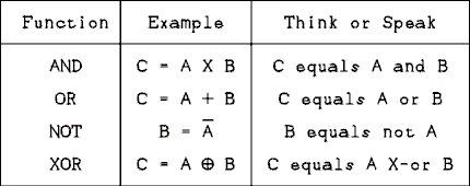
Figure 8.12 Table of Logic Functions and How to Speak Them.
For a verbal description click here.
Figure 8.13 Summary of Boolean Algebra Theorems.
For a verbal description click here.

Figure 8.13 lists some of the most important theorems in Boolean algebra. As you look over the table of theorems you will note some similarity to linear algebra. The last entry in the table is called DeMorgan's theorem. It is one of the most powerful and useful theorems for designing logic circuits.Example 8.2.
Use a truth table to prove that not A and B or A and not B = A X-or B.Solution:

For a verbal description click here.
QED.
Example 8.3.
Simplify the following Boolean expression.

Solution:
Factoring out an A we have

Using the theorem proven in Example 8.2 yields

Back to Fun with Transistors.
Back to Fun with Tubes.
Back to Table of Contents.
Back to top.
8.4 Combinational Logic Circuits.
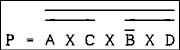
The term combinational logic is applied to any connection of logic gates which serves some specific purpose. For example, suppose that there is an experiment in which something in the apparatus could be damaged if certain switches were to be on at the same time. A system of gates could be used to shut down some critical part of the setup if an operator accidentally set the forbidden combination.Suppose that the equipment may be damaged if switches A and C are on at the same time or if switch B is off when switch D is on. The protection circuit P must be activated if A and C or not-B and D are on. In Boolean form the equation is,
Expression 8.1 cannot be simplified further. The circuit is shown in Figure 8.14. Gate 1 inverts the B input to form not B. Gate 2 forms the A AND C term while gate 3 forms the B AND D term. Gate 4 forms the final output. 

Figure 8.14 Realization of Boolean Expression 8.1.
For a verbal description click here.
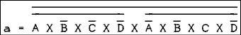
It was mentioned earlier that DeMorgan's theorem is very useful in creating logic circuits. The reason is this. The easiest type of gate for IC designers to design and manufacturers to make is the NAND gate. This is true for both TTL and CMOS logic families.Suppose that it is necessary to implement the following Boolean expression:
The first impulse would be to use the circuit of Figure 8.15a. However, DeMorgan's theorem extended for three variables states that, 
The expression D = not the quantity A X B X C may be implemented with a single 3 input NAND gate as shown in Figure 8.15b. 

Figure 8.15 DeMorgan's Theorem Is Used to Simplify Circuits.
For a verbal description click here.
The entire process of logic design is to start with a Boolean expression, simplify it and get as many NAND functions in it as possible, then convert the expression to a circuit.Example 8.4.
The output of a logic circuit is to be high (on) if A is on and B and C are off, or if A and C are on and B is off. Write the Boolean expression, simplify it if possible and then draw the circuit.Solution:
The initial form of the expression isThe initial uninformed solution might have been to implement the logic circuit based on the description in the example. A little Boolean algebra showed that the C input was redundant. In a simple circuit this wouldn't have made any practical difference. In a very complex circuit a redundant input could lead to use of a lot of unnecessary parts.

If we factor out an A and not B from each term we have

but not C or C = 1 and A and 1 = A; therefore, D = A and not B. The first impulse is to use an inverter to obtain the NOT-B term and a two input AND gate. Something you may not know is that gates do not come one per package. Two input gates come four per package. (The term DIP is often used. DIP stands for Dual Inline Package.) A two input NAND gate may be used as an inverter by tying its two inputs together and using them as the inverter's input. We can use one of the NAND gates as an inverter to obtain the NOT-B term, use another to perform the NAND function of A NAND NOT-B and then use another inverter to invert the output of the NAND gate and thereby convert it into an AND gate. The circuit is shown in Figure 8.16.

Figure 8.16 Solution to Example 8.4.
For a verbal description click here.
The solution to Example 8.4 ended up using three of the gates in a quadruple 2 input NAND gate. Such an IC costs less than 25 cents in TTL and less than 50 cents in CMOS.
Combinational logic circuits can get very complex as can the Boolean expressions which represent them. Such large projects are the province of design engineers who are experienced in such matters. The physics student should only attempt to design logic circuits if they are small and simple, as in Example 8.4.
Back to Fun with Transistors.
Back to Fun with Tubes.
Back to Table of Contents.
Back to top.
8.5 Flip-Flops and Counters.
The formal name for a flip-flop is a bistable device. It is a device which is stable in either of two states and will remain in whichever state it is in until it is forced into the other state where it will remain until again changed. Although this definition sounds simple, flip-flops come in a wide variety of shapes, sizes and colors. We will begin with the simplest.Switch Debouncing Flip-flop.
We are accustomed to thinking of mechanical switches as being either on or off. But if you look on a microsecond time scale, when a switch is turned on or off the contacts open and close several times before they finally settle down to the state in which it has been placed. If the switch is being used to turn a flashlight on and off the bouncing will make no difference and will not even be detectable by the user. But if the switch is being used to activate a logic circuit, operating the switch once may make the logic circuit "think" that the switch has been operated several times. The circuit of Figure 8.17 employs two NAND gates to generate one state change for each position change of the switch.
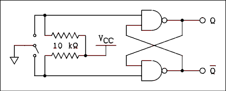
Figure 8.17 Switch Debouncing Circuit.
For a verbal description click here.
Suppose that the switch has just been thrown and is in transition between the two contacts. Neither switch contact is connected and so both switch contacts are pulled up to VCC by the 10 k ohm resistors. Suppose that Q is low (logic 0) and NOT-Q is high (logic 1). Both inputs to the upper gate are high which allows its output to be low. The lower gate has one input high and the other one low which makes its output high. So far so good, no contradictions.If the grounded swinger of the switch makes contact to the upper contact, one of the inputs to the upper gate will be pulled low. That will force its output to go high. The lower gate will now have a high on both inputs, which will make its output low. Thus, NOT-Q will be low (0). If the swinger loses contact on a bounce, the two outputs will remain in the same state. The swinger may bounce on the upper contact as many times as it likes, the state of the flip-flop consisting of the two gates will not change again until the swinger touches the lower contact.
Each time the switch is changed to the other position, the state of the flip-flop is changed by the first bounce of the switch contact. Subsequent bounces will not affect the state of the flip-flop. The contact will not bounce far enough to touch the other contact. The contacts are not made of rubber.
The R-S (Reset Set) Master-slave Flip-flop.
The logic diagram of an R-S master-slave flip-flop is shown in Figure 8.18. If the Ck (clock) input is low, gates 1 and 2 will both have high outputs and the master flip-flop consisting of gates 3 and 4 will remain in whatever state it was in; the states of the R and S inputs will have no effect on gates 3 and 4. If the Ck (clock) input is high, gates 1

Figure 8.18 Internal Logic Diagram of an R-S Flip-flop.
For a verbal description click here.
and 2 will be open, which means that the states applied to R and S will be transferred into the master flip-flop. The high on Ck will be inverted by the inverter and gates 5 and 6 will have low states on their inputs, which will close these gates. The outputs of gates 5 and 6 will be high, which means that the slave flip-flop will remain in whatever state it was in.It may seem impossible to ever transfer a logic state from the R and S inputs to the Q and NOT-Q outputs. Of course it is possible or the circuit would be useless. Let us start out by assuming that the Q output is low. Naturally the NOT-Q output is high. Referring to the flip-flop as a whole it is said to be in the zero state. Let us say that the S input is high, the R input is low and the Ck input is low. Because Ck is low the outputs of gates 1 and 2 will be high. The output of gate 3 must be low and gate 4 high. Gates 5 and 6 are open and these states are transferred through to gates 7 and 8. Now when the Ck input changes to high, gates 1 and 2 are opened and the states on R and S are inverted and transferred to the inputs of gates 3 and 4. A low on one of the inputs of gate 3 will cause its output to go high and gate 4 will have both of its inputs high, which will make its output low. The master flip-flop is now in the 1 state. With the Ck input high, gates 5 and 6 are closed and the slave flip-flop remains in the zero state. When the Ck input changes back to the low state, gates 1 and 2 are closed and the master flip-flop cannot be any further affected by the states on the R and S inputs. The level shift causes the inverter to change states at a lower voltage than gates 1 and 2. On a negative transition, gates 1 and 2 are closed before gates 5 and 6 are opened. Thus there is an approximate 20 nanosecond period when both sets of gates (1 and 2) and (5 and 6) are closed and the R and S inputs are never connected directly to the Q and NOT-Q outputs. With the Ck input in the low state, gates 5 and 6 are opened and the 1 state of the master flip-flop is transferred into the slave flip-flop. Thus the state of Q is now high and NOT-Q is low. If the S input is high and R is low the flip-flop will be Set to the 1 state (Q high and NOT-Q low) and when R is high and S low the flip-flop will be Reset to the zero state. The states of Q and NOT-Q will change only when the Ck input changes from high to low. After the states of Q and NOT-Q have changed to match the states of S and R, additional clock transitions have no effect on the state of the outputs.
If R and S are both low, the flip-flop will remain in its previous state. The outputs will not change states on the clock transition. If both R and S are high, the flip- flop of gates 3 and 4 will be forced into an undefined state and when the clock goes low it will be released from that state and will randomly fall into one of its two stable states. The ending state cannot be predicted. A given IC may always fall into the same state but a different IC may always fall into the other state. Yet another IC may randomly fall into one or the other state.
Most flip-flop ICs have direct set and clear inputs. These inputs will override all other inputs and force the flip-flop into the 1 (set) of 0 (clear) states. The logic involved makes the circuit look more complicated because of the increased number of inputs to gates 3, 4, 7 and 8. A student with a firm grasp of the subject of logic could figure out how to add direct set and clear to this circuit.
The J-K Flip-flop.
If the R-S flip-flop is cross wired (Q to R and NOT-Q to S) an interesting thing happens. Suppose that the flip-flop is in the zero state (Q = 0 and NOT-Q = 1). This means that S has a high applied and R has a low. When a negative edge of the clock occurs, the flip-flop will be loaded with a 1. Following the negative-going clock the R input has a high applied and the S has a low applied. On the next negative-going clock edge the flip-flop will be loaded with a zero. The flip-flop will change its state on every negative-going edge of the clock signal.Now the importance of the level shift becomes evident. On a positive edge of the clock, gates 5 & 6 are closed before gates 1 & 2 are opened. On a negative edge gates 1 & 2 are closed before 5 & 6 are opened. If the R and S inputs were to be connected directly to the outputs even for a few tens of nanoseconds the circuit would most likely oscillate and the ending state would be completely random.

Figure 8.19 Internal Logic Diagram of a J-K Flip-flop.
For a verbal description click here.
If we make gates 1 and 2 into 3 input gates we have a J-K flip-flop as shown in Figure 8.19. The J-K flip-flop behaves differently from the R-S flip-flop in regard to what happens when J and K are high. In an R-S flip-flop when R and S are high the result is unpredictable. In a J-K flip- flop when J and K are high the flip-flop will change states on every negative edge of the clock input. The process of changing states on every clock is often called toggling. A flip-flop which has been permanently wired to change states on every clock pulse is often called a toggle flip-flop.If J is high and K is low the flip-flop will be set to the 1 state on the next negative edge of the clock. If J is low and K is high the flip-flop will be set to the zero state on the next negative edge of the clock. If both J and K are low the state of the flip-flop will remain unchanged.
The Type-D (Data Storage) Flip-flop.
In order to store a bit (binary digit) in an R-S or J-K flip-flop it is necessary to place one of the inputs high and the other one low. Since the two inputs are always in opposite states the natural thing to do is to connect an inverter in the circuit as shown in Figure 8.20a. When a flip-flop has been internally wired in this way it is symbolized as in Figure 8.20b. Notice first of all that the internal logic diagram has been replaced by a rectangle. If a logic high (1) is placed on the D input, the next negative edge will cause the flip-flop to assume the 1 state (Q = 1 and NOT-Q = 0). If a logic low (0) is placed on the D input, the next negative edge on the clock will cause the flip-flop to assume the zero state (Q = 0 and NOT-Q = 1). Once the data bit has been stored in the flip-flop, subsequent clock pulses will just keep loading the same data again and again. If the data does not change between clock pulses the state of the flip-flop will not change.

Figure 8.20 D-type Flip-flop from J-K Flip-flop.
For a verbal description click here.
The Cl connection at the bottom of the rectangle and the S connection at the top are direct clear and set inputs respectively. This S is not the same as the S input on an R-S flip-flop. Clear and set inputs are usually active low, which means they are normally high and to clear the flip-flop the Cl input should be pulled low for a few tens of nanoseconds. To set the flip-flop the S input should be pulled low. In the case of TTL an input which is left open will automatically go high. A CMOS input should never be left open; on a CMOS flip-flop the Cl and S inputs must be tied to VCC through either a wire or a 10 k ohm resistor.Binary Counter.
Figure 8.21 shows the diagram and truth table for a 4-bit binary counter. There is an inherent conflict between the way we draw circuits and the way we write numbers. The standard way of drawing circuits is to have the signal flow from left to right. That places the least significant bit on the left. The way we write numbers is to have the least significant bit on the right. This contradiction cannot be defined away. We must simply live with it.The input to the counter may be irregular or regular pulses as indicated along the top of the figure. All unconnected inputs to the flip-flops are assumed to be logic high. Every time a flip-flop receives a negative-going edge, its state will change. See the table in the figure.

Figure 8.21 4-Bit Binary Counter and Its Truth Table.
For a verbal description click here.
Every time the input changes from high to low, flip-flop A will change states. Every time flip-flop A changes from a 1 to a 0, flip-flop B will change states and so on. If the counter starts from zero (all bits zero) the count at any time will equal the number of negative edges which have occurred in the input signal. The number is of course expressed in binary. The number of flip-flops in the counter may be arbitrarily large. The largest number NL a given counter can contain isNL = 2N - 1 (8.4) where N is the number of flip-flops in the counter.If the input to the counter is a square wave it has a definite frequency. In this event the output of the counter also has a definite frequency. The output frequency is given by
fO = fIN / 2N (8.5) where fO is the output frequency, fIN is the input frequency and N is the number of flip-flops in the counter. Thus we have a means of changing (lowering) the frequency. With a simple binary divider the input frequency may only be divided by 2N where N is an integer.When a binary counter is used to divide frequencies it is called a frequency divider. Divide ratios can be other than 2N but the circuitry becomes more complex. Noninteger divide ratios are even possible but the circuitry becomes very complex.
Example 8.5.
The input frequency to a 9 stage (9 flip-flops) binary counter is 225,280 hertz. What is the output frequency?Solution:
fO = fIN / 2N = 225,280 / 29 = 440 hz.
The Decade Counter.
When binary numbers were introduced it was said that it was difficult to make electronic circuits which could count in decimal. In the age of the IC it is easier than it was in the vacuum tube age. Computer hardware designers still prefer to use binary but in stand alone digital instruments such as digital clocks, frequency counters and digital voltmeters the decade counter is king.The circuit employs a number system known as binary coded decimal (BCD for short). Figure 8.22 shows how to count from 0 to 12 in BCD. Each decimal digit is represented by 4 binary digits (bits). Four bits of binary can normally express numbers as large as 15 (1111) but in BCD the highest allowed count is 9 (1001). Binary counts higher than 1001 are not allowed. Notice that in Figure 8.22 when the units count reaches 9 it resets to 0 and a 1 is placed in the tens column.
This system of counting requires more bits than a comparable binary counter. For example a 3 digit BCD counter can count to 999 and requires 3 digits x 4 bits per digit = 12 bits. A binary counter which can count to 1023 requires only 10 bits. The extra bits are well worth the tiny increase in cost. The circuitry to readout a 10 bit binary counter in decimal is far more complex and expensive than the couple of extra bits required for making BCD counters.
In order to implement BCD in hardware it is necessary to wire together 4 flip-flops in such a way as to count from 0 to 9, which is the same thing as dividing the input frequency by ten. Ten can be factored as 2 x 5. A single flip-flop can handle the divide by 2. Three flip-flops and some gates are used to accomplish the division by 5.
Decimal Tens Units 00 0 0 0 0 0 0 0 0 01 0 0 0 0 0 0 0 1 02 0 0 0 0 0 0 1 0 03 0 0 0 0 0 0 1 1 04 0 0 0 0 0 1 0 0 05 0 0 0 0 0 1 0 1 06 0 0 0 0 0 1 1 0 07 0 0 0 0 0 1 1 1 08 0 0 0 0 1 0 0 0 09 0 0 0 0 1 0 0 1 10 0 0 0 1 0 0 0 0 11 0 0 0 1 0 0 0 1 12 0 0 0 1 0 0 1 0 Figure 8.22 BCD Counting from 0 to 12.
A practical decade counter is made up of 4 flip-flops, as shown in Figure 8.23. This circuit consists of a count- to-one (divide by 2) and a count-to-four (divide by 5) circuit. The count-to-one section consists of flip-flop A. The count-to-four circuit consists of flip-flops B, C, D and two gates.
Whenever a TTL (transistor transistor logic) input is left open, it assumes the high logic state. (This is not recommended in circuits constructed in the laboratory.) The J and K inputs on flip-flop A are open; consequently, they both have high logic states or 1s applied. If a J-K flip-flop has 1s on both J and K inputs, the flip-flop will change states every time the clock input goes from a logic 1 to a logic 0. If there is one cycle at the output for every two cycles at the input, you have a divide by 2 counter.
The divide by 5 is not so simple. If 3 flip-flops are connected with the Q output of one going to the Ck input of the next, the counter will be a count to 7 or divide by 8. To make this counter divide by 5 instead of 8 requires some trickery.

Figure 8.23 Decade Counter and Its Truth Table.
For a verbal description click here.
The truth table which accompanies Figure 8.23 has all of the numbers written backward. This should aid in understanding the circuit. The column of binary digits for a given flip-flop is under that flip-flop.Starting out with all flip-flops set to zero, the NAND gate will have a 0 and a 1 on its inputs. Its output will be a 1. This 1 when applied to the J input of F-F B will allow it to change states on every clock pulse. When the count in F-Fs B, C and D reaches 0 0 1 (binary 100) both inputs of the NAND gate will be 1s and the output will be 0. The 0 on the J input of F-F B will prevent it from changing states on the next clock pulse. Because there is no change in the state of F-F B, there will not be any trigger pulse delivered to F-F C and it will remain in the 0 state.
The AND gate gets its inputs from F-Fs B and C. The output of the AND gate will be 0 as long as B or C is 0. The 0 applied to the J input of F-F D will inhibit it from changing states and it will remain in the 0 state. When B and C are both 1s, there will be a 1 on the J input of F-F D and it will change states on the next clock pulse.
Note that the clock pulses are connected to F-Fs B and D. The clock pulse which caused D to change from 0 to 1 will cause B to change from 1 to 0. This change on the Q output of F-F B will cause F-F C to also change from 1 to 0. F-F B is now inhibited from changing states. As we have already seen, F-F D had a 1 on its J input before the clock transition and so the next transition will cause F-F D to change from 1 to 0. We now have all flip-flops back in the 0 state and we are ready for another counting cycle.
This circuit is almost never implemented with separate J-K flip-flops and logic gates. A decade counter integrated circuit is normally used. Different manufacturers implement the counter in different ways and many of them will not even tell us how they do it. It may be done this way or some other way; we don't know.
Variable Modulus Counters.
The modulus of a counter is that number by which it will divide an input frequency. For a counter of modulus N, for every N pulses sent to the counter it will deliver one pulse. The modulus of a 4-bit binary counter is 16, that of a decade counter is 10 and that of the B, C and D flip-flops of a decade counter is 5.As illustrated by the decade counter it is possible to develop systems of flip-flops and gates to give any desired modulus. Such systems are hard-wired and cannot be changed by the equipment operator. There are counters whose moduli can be changed by the operator.
A very common variable modulus counter uses the up-down decade counter. Each IC has a count-up and a count-down input. There are also carry and borrow outputs. The carry output is wired to the count-up input and the borrow output is wired to the count-down input of the next most significant digit counter. These counters also have a set of direct load inputs which permit data to be loaded into the counter. A "load enable" input on the IC causes data which is presented at the data inputs to be loaded into the flip-flops of the counter.
When the input signal is applied to the count-down input of the least significant digit the borrow output of the most significant digit will go low only when all digits in the counter are zero. The rest of the time this output is high. If this output is connected to the load enable inputs of all of the other digits in the counter the data will be loaded whenever the counter arrives at zero. The data are loaded when the load enable input is low.
The sequence of events is this: the counter counts down to zero, the data are loaded, and the counter counts down to zero again. The modulus of the counter is equal to the number contained in the data which is loaded. If the data are changed, the modulus of the counter is changed.
One way an operator can interact with such a counter is by means of thumb-wheel switches. Each switch has ten positions. When the switch is set to a given position a digit (0 through 9) will show in a window to indicate to the operator the position selected. The switch has four contacts which generate the BCD code corresponding to the digit selected. These switches are designed so they may be placed side by side to allow an operator to set a decimal number on the switches. The outputs of the switches are the BCD code of the number selected. If the switches are connected to the data inputs of the up-down counters, the switches may be used to select the modulus of the counter. The usefulness of such a variable modulus counter will be shown in the next chapter.
It is possible to achieve a noninteger modulus by using combinational logic to set the modulus, as was done for the divide-by-five circuit. Such a circuit may be arranged so that a logic level on one of the gates will change the modulus of the counter. The level on this modulus control input may be rapidly switched to obtain an average modulus which is between integer values. Such a counter must be followed by several divide-by-two flip-flops in order to average out the frequency variations and give a true single frequency output. Circuits of this kind are used in an IC called a "top octave generator". This IC uses a quartz crystal (externally connected) and divides it down to deliver simultaneously all twelve of the musical notes in the top octave of the standard piano keyboard. In each lower octave the frequencies of the notes are half of those in the next higher octave. Simple binary dividers may be used to generate the rest of the notes on the keyboard.
By the way, if you want to amaze a guitar-playing friend by telling him or her the frequencies of the musical notes, it is easy using a calculator. The frequency of the note A above middle-C is 440.000 hz. The notes comprise a geometric series with the twelfth root of two being the factor. Use the YX key on your calculator to raise 2 to the 1/12 power and store the result in memory. Key in 440. To move down the musical scale, recall and divide. To move up the scale, recall and multiply. If you work your way down the scale to middle-C you will find its frequency to be 261.6256 hertz. You may well have read in an elementary physics book that middle-C has a frequency of 256 hertz. The best information available to the writer indicates that musicians changed the standard of tuning sometime early in the 20th century. They forgot to tell the physicists. Meanwhile, any physicists writing a book would look up the frequency for middle-C in the book he had used as a student which was written by someone who looked it up in a book he had used as a student and so on. This is how misinformation can be passed down from one generation to the next.
Back to Fun with Transistors.
Back to Fun with Tubes.
Back to Table of Contents.
Back to top.
8.6 Displaying the Count.
In any digital instrument it is necessary for the contents of the counter to be displayed in some way for an operator to read. Figure 8.24 shows the block diagram of a single digit of the readout system for a decade counter.
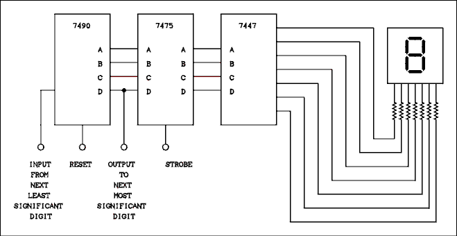
Figure 8.24 Decade Counter, Latch, Decoder and Display.
For a verbal description click here.
The numbers in the blocks are type numbers of specific ICs. The 7490 is the decade counter. Such a counter is in the middle of a chain of similar decade counters. The 7475 is a 4-bit memory consisting of 4 type D flip-flops. The purpose of the "strobe" input is to cause the data in the decade counter to be loaded into the memory. The purpose of the memory is to remember the count while a new count is being accumulated. The sequence of events is this. The count begins and the decade counters count up from zero. When the count has finished, the "strobe" inputs of all of the memories is pulsed which stores the data in the memory. The counters may then be reset (to zero) and a new count begins while the memory holds the previous count.The contents of the memory are fed to the 7447 which is a decoder-driver. This IC uses combinational logic to convert the BCD code from the memory to the proper pattern to display numerals on the 7-segment display. The outputs of the decoder-driver are BJTs which are "on" to light a display and "off" to keep it dark. These BJTs are capable of switching enough current to drive almost any display which may be used.
The display itself consists of 7 light emitting diodes (LEDs). These LEDs have an I-V curve similar to any other diode. The full 5 volt power supply cannot be applied across the LEDs in the display. There must be a current limiting resistor in series with each LED in the display. A typical value is 220 ohms. Some other types of decoder-drivers have these resistors built in to the IC.
There must be one of these circuits for each digit to be displayed. An 8-digit display would have eight 7490s, eight 7475s, eight 7447s, fifty-six resistors and eight displays.
Back to Fun with Transistors.
Back to Fun with Tubes.
Back to Table of Contents.
Back to top.
8.7 Multiplexed Displays.
The term LSI means large scale integration. It is LSI which has made the pocket calculator possible. One problem with LSI is the number of pins necessary to connect to the display. A ten-digit calculator needs eighty pins to control the numeric display and the decimal points. That is far too many for a reasonable size for the IC and the calculator it is used in.A way to save pins is to multiplex the display. Instead of connecting the anodes of the LEDs in the display to the +5 volt line, they are connected to the collectors of PNP switching transistors. A ten-digit calculator needs ten control lines, one for each digit. All of the segment cathodes are connected in parallel. For example the top segments in all ten of the digits are connected together. All ten of the decimal point cathodes are connected together. That means that there are 8 lines, one for each segment and 1 line for the decimal points. That makes 10 digit control lines plus 8 segment control lines for a total of 18 lines to control 10 digits, instead of 80 as would be the case for individual segment connections. Also only 8 resistors are needed for current limiting.
The way in which this works is as follows. The PNP transistors in the digit anodes can turn an entire digit on or off. The first digit is turned on (all others are off) and the pattern of bits is applied to the segment lines to display the number in the first digit. The first digit is turned off and the second digit is turned on. The data on the segment lines is changed to that of the number in the second digit. The process repeats until all of the digits have been illuminated and then the process begins again. Even though only one digit is on at a time, the eye perceives a continuous display of all digits. The scanning of the displays may occasionally be observed when a calculator is shown on television. The field rate of the TV scanning may "strobe" with the scanning rate of the calculator's display.

Figure 8.25 Multiplexed 4 Digit Display.
For a verbal description click here.
The display will appear to flicker and if the frequency of the display scanning is just right it may even be seen to scan in order. If you ever gain access to a stroboscope, (not to be confused with a strobe light), you may want to put your calculator under it and see if you can find the scanning frequency.The keyboard of a calculator s another problem. Many calculators have 40 to 50 keys. If there had to be one pin on the IC for each key, calculators would be a lot larger and more expensive than they are.
The keyboard is divided into rows and columns (not necessarily related to their physical placement on the calculator). The keyboard is scanned. For example a calculator having 64 keys does not need 64 pins to connect the keys. The keyboard is electrically arranged into an 8 by 8 matrix and connected as shown in Figure 8.26. Each switch is a key on the calculator. The calculator IC may send pulses out on the column lines one at a time and monitor the row lines for returned pulses. When a switch is closed only one of the 8 column pulses will be received and it will be received on only one row line. That gives an unambiguous way for the chip to know which one of the switches was closed. The calculator IC needs only 16 pins for the keyboard instead of 64.
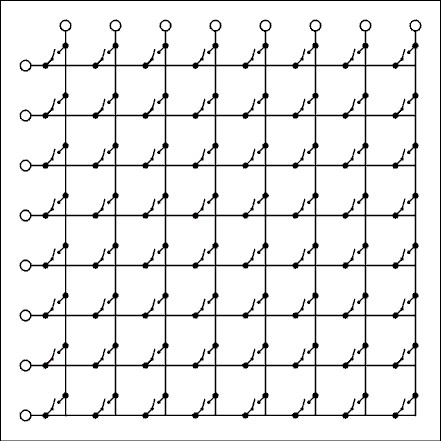
Figure 8.26 Multiplexed Calculator Keyboard.
For a verbal description click here.
Back to Fun with Transistors.
Back to Fun with Tubes.
Back to Table of Contents.
Back to top.
8.8 Digital to Analog Converter.
A number held in a digital counter or memory is just a number. Like any number it represents only what we humans imagine. In and of itself it represents nothing. However, a circuit may be constructed which will convert a digital number to a proportional voltage. Such a circuit is called a digital to analog converter (DAC).A digital to analog converter (DAC) which is easy to understand is shown in Figure 8.27. Suppose that the output of the digital buffers is 5 volts if the input is a logic 1 and zero volts if the input is a logic zero. If the most significant bit (MSB) is 1 the 10 k ohm resistor will supply a current of 0.5 mA to the summing node of the op amp. The next bit will cause a current of 0.25 mA to be delivered to the summing junction, the next a current of 0.125 and so on. If the least significant bit (LSB) is a 1 the current from it is 7.8125 uA. An infinite number of bits would bring the total current (all bits on) up to 1 mA. The condition of all bits on (1) is the full-scale condition. The 5 k ohm feedback resistor will cause the op amp to have a full-scale output voltage of -5 volts. When converting binary to decimal each bit has twice the value as the bit to its right. In the case of the digital to analog converter each bit supplies twice the current as the next least significant bit. The op amp causes all of these currents to be summed and converted into a negative voltage. If a positive output is desired another op amp may be connected as a unity-gain inverter.

Figure 8.27 Simple Digital to Analog Converter.
For a verbal description click here.
Although this circuit is easy to understand it doesn't work very well. The problem is the resistors. If the resistors are not exactly right on value the converter will not yield uniform steps as the binary number is incremented. Take the case of stepping from 63 to 64. The number 63 has the 6 least significant bits on. When this number changes to 64, 6 bits turn off and a single bit takes its place. The 10 k ohm resistor must supply a current which is exactly 7.8125 uA larger than the current supplied by the combination of the 6 other resistors. (The smallest possible step in the output of a DAC is the value of the least significant bit.) Errors in resistors are random and, if the particular resistors have errors such that the 20 k ohm is a little low and the 10 k ohm is a little high, incrementing the binary code from 63 to 64 could actually result in a reduction of the output voltage instead of an increase. As the number of bits increases the smallest steps become smaller and the requirements on resistor tolerance become impossibly tight.Another problem is the wider range of resistor values required by this type of converter. The values in this example circuit range from 10 k ohm to 640 k ohm and this is only a 7-bit converter. A 16-bit converter which has a lowest value resistor of 1 k ohm would have to have a highest value resistor of 32.768 M ohms. Maintaining the necessary tolerances over such a wide range of resistance is impossible.
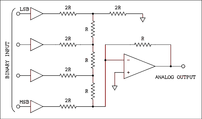
Figure 8.28 Ladder Network Digital to Analog Converter.
For a verbal description click here.
Figure 8.28 shows a digital to analog converter which will work. The figure shows only 4 bits but the circuit may be extended to as many bits as desired. If the MSB is the only bit to be on, the output voltage will be half of the power supply voltage. That is as it should be because the MSB always represents half of the (largest - 1) number that a given binary number can represent. The MSB is 1/2 scale. The next bit is 1/4 scale, the next 1/8 scale and so on.Although it is not exactly cheap, it is possible to make a large number of resistors all of the same value. The ladder network is supplied in a package which looks like an IC. The resistors were all made at the same time on a common substrate. The resistors indicated as 2R are just two of the resistors connected in series during the manufacturing process. The actual value R may vary by as much as 10% from unit to unit but within a single unit the resistors are all identical to within a small fraction of a percent. A very high precision DAC may be constructed using a ladder network.
The diagrams show noninverting buffers as the drivers for the DAC. Ordinary TTL cannot be used at all and even CMOS is not good enough for high accuracy DACs. The problem is the voltage that the output of the buffer goes up to when its output is a logic 1. TTL is only guaranteed to go up to 2.4 volts. CMOS does quite a bit better but when its output is loaded by a resistor network the output of a buffer may not make it all of the way to ground for a logic zero or all the way to VCC for a logic 1. Designers of DACs go to great length to design switching circuits which will be at zero volts for a binary zero and at VCC for a logic 1. In addition the VCC supply must be very precisely regulated.
As a physicist you will never have to worry about any of the above. DACs are available in IC form ranging in bit count from 8 to 20 and in price from $3.95 to several hundred dollars. The data sheet for the particular DAC IC to be used must be consulted in order to use it properly.
Back to Fun with Transistors.
Back to Fun with Tubes.
Back to Table of Contents.
Back to top.
8.9 Analog to Digital Converter.
The process of converting a voltage to a digital number is called analog to digital conversion. The voltage may be converted to a BCD (binary coded decimal) number as is done in a digital multimeter or to a binary number if the data are to be fed to a computer for processing.Analog to digital converters (ADCs) like DACs come in IC packages. They are available in two basic forms, slow and less expensive and fast and more expensive. The slow kind are dual slope integrators and the fast are successive approximation type. Both types can be quite accurate.
Dual-slope Integrator ADCs.
The dual-slope converter is most often used in digital multimeters. Its output is usually in BCD form for easy decimal readout. The typical speed for this converter is about 4 samples per second. That is plenty fast enough for a slow human to take in.In the circuit of Figure 8.29 the input voltage must be negative. In a complete voltmeter there are circuits which allow the input voltage to be positive or negative. A flip- flop indicates the polarity of the input voltage. To show this extra circuitry would add to the circuit complexity while adding nothing to the reader's understanding.

Figure 8.29 Dual-slope Integrator ADC.
For a verbal description click here.
In the circuit of Figure 8.29 the switches S1, S2 and S3 are not mechanical but electronic switches which are controlled by the block labeled "control logic". The sampling cycle starts by closing switch S1 to discharge the capacitor. S1 is opened and S2 is closed which signals the beginning of time period T1. The output voltage of the integrator begins to go positive because the input voltage is negative. The slope of the line is determined by the magnitude of the input voltage as indicated by the waveform drawings in the figure. At the end of T1 the output voltage of the integrator is proportional to the magnitude of the input voltage. At the end of T1 S2 opens and S3 closes, signaling the start of T2. The reference voltage is the negative of the full-scale voltage of the converter. When T2 begins, the control logic opens the AND gate by placing a logic 1 on the lower input. The upper input of the gate already has a 1 on it from the output of the comparator.The symbol for a comparator looks like an op amp and there are similarities. A comparator is a device which can have an analog input and a digital output. It may be thought of as a one-bit analog to digital converter. If the noninverting input is more positive than the inverting input the output will be a logic 1. If the inverting input is more positive than the noninverting input the output will be a logic zero.
In the circuit of Figure 8.29 the inverting input of the comparator is grounded and the positive output of the integrator is applied to the noninverting input. The output of the comparator is a logic 1. Clock pulses from the clock are now passed to the counter. The counter counts clock pulses for the duration of T2. The time period T2 ends when the output of the integrator reaches zero. As the two different waves in the figure indicate, the higher the magnitude of the input voltage the longer T2 is and the larger the number of clock pulses counted. When the output of the integrator reaches zero the AND gate is closed because the output of the comparator has switched to a logic zero. The control logic is also notified and it initiates a number of steps. S3 is opened, the contents of the counter are loaded into the display memory and the counter is reset to zero. Now S1 is closed and the entire cycle starts over again.
You may be thinking that a much simpler way would be to let the reference voltage be integrated until it equals the input voltage and let the counter count clock pulses during this time. If you did think of this method, go to the head of the class. It shows that you are thinking. The calibration of such a single-slope integrator is very dependent on the value of the capacitor. Capacitors have a rather bad habit of changing capacitance as temperature changes. In a dual-slope integrator the capacitor is used twice and errors in the value of the capacitor are partially canceled out. This partial error cancellation is the primary reason for using a dual-slope integrator instead of a single slope integrator.
Successive Approximation ADC.
Successive approximation converters are very fast, ranging in speed from several hundred samples per second to several million samples per second. In bit count they range from 8 to 20 and in price from $3.95 to several hundred dollars. Because of their great speed they are most often used in association with microprocessors. They usually have binary output.The diagram of a successive approximation ADC is shown in Figure 8.30. You will notice that contained within the analog to digital converter (ADC) is a digital to analog converter (DAC). The comparator compares the output of the DAC with the input signal and sends its output signal to the control logic. The wide lines on the diagram labeled "data bus" and "control bus" are a shorthand way of drawing many individual connecting lines. In the case of a 16 bit converter, there would be 16 lines connecting the control logic block to the binary register and 16 lines connecting the binary register to the DAC. It is pointless to draw 16 lines when everyone knows that they are all going to the same place.

Figure 8.30 Successive Approximation ADC.
For a verbal description click here.
One very simple way in which this circuit could be used is to start the binary register (used as a counter) at zero, count up until the comparator changes states and then stop. That method works fine provided you are not in a hurry. If the input signal is near full-scale, as many as 65 thousand clock pulses would be required to complete a conversion in a 16 bit converter. The conversion time is dependent on the magnitude of the input signal. An input signal which is near zero takes fewer clock pulses and, therefore, less time than an input signal which is near full-scale.The successive approximation system works much faster. The difference between a binary counter and a binary register is that a binary register can be loaded with data in many ways. In the binary register used here each bit can be changed individually. The binary register starts with all bits set to zero. The control logic sets the most significant bit (MSB). If the comparator changes states because the output of the DAC is larger than the input signal, the bit is reset. Otherwise it is left set. The next least significant bit is tried in the same way: if turning it on makes the output of the DAC greater than the input the bit is turned off, if the DAC's output is less than the input, the bit is left on. If it is necessary to turn a bit off the same clock pulse which turns that bit off can turn on the next bit. In the case of a 16 bit converter only 16 clock pulses are required to complete a conversion.
A microprocessor could easily be programmed to perform the function of the control logic. A microcomputer which is equipped with a DAC for the purpose of playing music needs only the addition of a comparator feeding into a game paddle port and it can be used as an ADC.
Single IC converters use combinational logic to accomplish the job of the control logic. Such converters can be made very fast indeed.
Back to Fun with Transistors.
Back to Fun with Tubes.
Back to Table of Contents.
Back to top.
8.10 The 555 Timer.
The 555 timer resides in a kind of twilight zone between analog and digital. It incorporates elements of both but it is more digital than analog so it is included here.A 555 timer is basically a monostable Multivibrator or one shot. In this device it is stable in one state where it remains until triggered. Upon being triggered it changes to the other state where it remains for a length of time determined by an RC time constant and then returns to the stable state. Both the TTL and CMOS logic families have one shots in the line. Some are retriggerable which means that if another trigger pulse arrives before the RC has timed out the time period will start over. Others are not retriggerable which means that trigger pulses are ignored while the RC is timing out. Some can be wired for either kind of behavior.
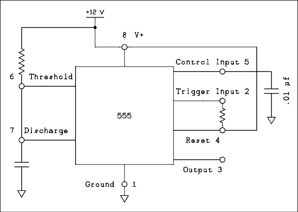
A 555 is not retriggerable and requires the addition of an external transistor to make it into one. The internal block diagram is shown in figure 8.31. Figure 8.32 shows a 555 timer wired as a one shot.
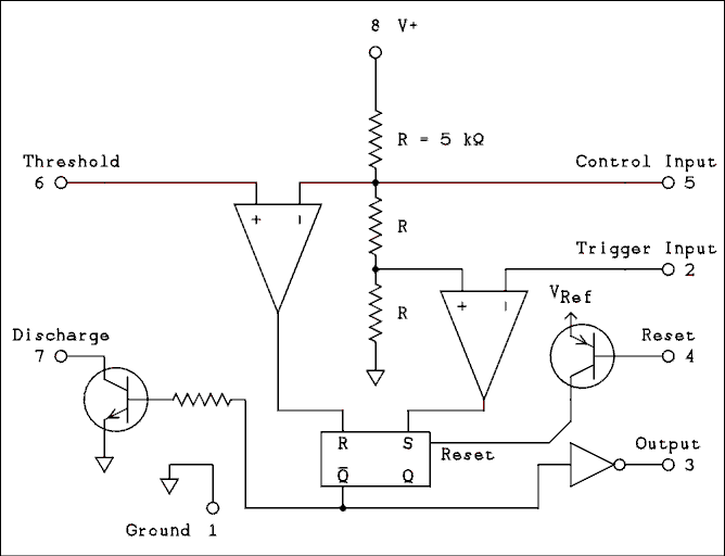
Figure 8.31 Internal Block Diagram of the 555 Timer.
For a verbal description click here.
Figure 8.32 One-shot, Pulse Stretcher.
For a verbal description click here.
In the stable state the trigger input is held high by the resistor. The output is low and the not Q input is high. This holds the transistor on which keeps the capacitor discharged. The trigger input goes to the inverting input of the comparator so the S input of the flip flop is low. The discharge and threshold pins are tied together so the noninverting input of the other comparator is low making the R input of the flip flop low. With R and S both low the flip flop will not change states.The trigger pulse would be negative and short. A negative pulse on the inverting input of the comparator drives the output positive setting the flip flop. The not Q goes low and the output goes high. The discharge transistor is turned off and the capacitor begins to charge through the resistor. Note the network of equal value resistors in the center. The comparator on the right has its noninverting input held at 1/3 of VCC. The one on the left has its inverting input held at 2/3 of VCC. As long as the voltage across the capacitor is less than 2/3 VCC The R input of the flip flop remains low. When the voltage reaches 2/3 VCC the R input goes high and the flip flop is reset. The output returns to low, the discharge transistor is turned on, discharging the capacitor and the timer is back in its stable state.
After the timer has been triggered and before the RC circuit has timed out additional trigger pulses will have no effect. Such pulses would set the flip flop but it is already set.
There are many possible uses of this circuit but one could be as a pulse stretcher to turn on an indicator light. Suppose part of an experiment delivers pulses that are so short that even if they were used to turn on an L E D the flash would be too short to perceive. A requirement is that the operator must know when such pulses occur. The narrow pulses could be applied to the input of a circuit like that of figure 8.32 with its R and C values selected for a timeout of say 1 second. The timer could be used to light a lamp and sound a buzzer to be sure to get the attention of the operator.
The time that the output remains high is given by,
T = 1.1 R C (8.6) Oscillator Circuit.
In the circuit of figure 8.33 The capacitor is connected back around to the trigger input so the timer will trigger itself. There is a resistor connected between the capacitor and the discharge terminal so the capacitor will take some time to discharge.When the output goes low and the discharge transistor is turned on the capacitor discharges through R2. When the capacitor voltage reaches 1/3 VCC the flip flop is set and the discharge transistor is turned off. The capacitor then charges through the series combination of R1 and R2. When the voltage reaches 2/3 VCC the flip flop is reset and the cycle starts over.
It is impossible to get square waves out of this circuit because the capacitor is charged through 2 resistors in series and discharged through one. The Frequency is given by,
f = 1.46 / [(R1 + 2R2)C] (8.7)

Figure 8.33 Oscillator with Pulse Train Output.
For a verbal description click here.
Figure 8.34 Oscillator with Square Wave Output.
For a verbal description click here.
The circuit of figure 8.34 will solve this problem. When the capacitor is charging the diode effectively shorts out R2, causing the capacitor to charge through R12 alone. If the circuit is operated from 5 volts it will most likely be necessary to make R1 one 5% step less than R2 to account for the effect of the forward voltage drop across the diode. If the resistors are the same value the frequency is given by,f = 0.730 / RC (8.7) Back to Fun with Transistors.
Back to Fun with Tubes.
Back to Table of Contents.
Back to top.
8.11 Problems.
- Convert 1110111 to decimal.
- What is the sum of 101011 and 1101?
- What are the names of the gates whose truth tables are given here?
(a) A B C OUTPUT 0 0 0 1 0 0 1 1 0 1 0 1 0 1 1 1 1 0 0 1 1 0 1 1 1 1 0 1 1 1 1 0
(b) A B C OUTPUT 0 0 0 1 0 0 1 0 0 1 0 0 0 1 1 0 1 0 0 0 1 0 1 0 1 1 0 0 1 1 1 0 - Write the truth table for the circuit of Figure 8.35. Suggestion: Make columns in your truth table for the outputs of gates 1, 2 and 3. These tree columns will then be the inputs for gate 4.

Figure 8.35 Combinational Logic Circuit For Problems 4 and 5.
For a verbal description click here.
- Write the Boolean algebra expression for the circuit of Figure 8.35. Do not attempt to simplify it.
- Convert Expression 8.1 into NAND gates.
- Reduce the expression below to all NAND functions.

- Add direct Set and Clear inputs to the master-slave R-S flip-flop of Figure 8.18. Tell what the states of these inputs must be for normal operation and what state will cause a set or clear. You may add inputs to any of the gates if necessary.
- What is the largest number that a 13-bit binary counter can contain? Express your answer in decimal without using exponents.
- If the input frequency to a 12-bit binary counter is 3,579,545 hz, what is the output frequency?
- A frequency divider consists of a divide by 5 module followed by a divide by 7 module which is followed by a divide by 13 module. What is the division ratio of the entire system?
- In an 8-digit frequency counter the decimal points are to be turned on and off by circuitry within the counter chip. If the display is multiplexed, how many pins are required to connect the display to the counter IC?
- When a 555 timer is used as a monostable what should be the value of C to give a 1 second pulse if the resistor is 150 k ohms?
- When a 555 timer is used as an oscillator without a diode what should be the value Of the capacitor to give a frequency of 1 hertz if R1 = R2 = 220 k ohms?
- When a 555 timer is used as an oscillator with a diode what should be the value Of the capacitor to give a frequency of 1 hertz if R1 = R2 = 330 k ohms?
Back to Fun with Transistors.
Back to Fun with Tubes.
Back to Table of Contents.
Back to top.
8.12 Answers to Problems.
- 119
- 111000
- (a) NAND, (b) NOR.
- Truth table.
A B C OUTPUT 0 0 0 0 0 0 1 1 0 1 0 0 0 1 1 0 1 0 0 1 1 0 1 0 1 1 0 0 1 1 1 1
- The unsimplified expression is,

For a verbal description click here.
- The NAND gate expression is,
For a verbal description click here.
- The answer is...
For a verbal description click here.
- For normal operation both SET and CLR must be high. Pulling the SET input low will set the flip flop and pulling the CLR input low will clear it.

For a verbal description click here.
- 8191.
- 873.912 Hz.
- 455
- 16.
- 6.06 micro farads.
- 2.21 micro farads.
- 2.21 micro farads.