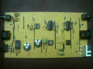
Gap control
For normal constant-gap scanning, the height level is driven by a feedback signal derived from the tunnel current itself. The main board receives a signal It+Vb from the tunnel pre-amp. The Vb and the Iref+Vb voltage levels can be set conveniently throught the graphical interface provided by the software. The error signal is obtained by subtracting the incoming It+Vb from the Iref+Vb signal dictated by the IO card. This is done using an INA101HP instrumentation chip. Some extra gain may be derived from this stage by making use of the nonlinear gain potentiometer.
The next stage, based on an OPA27GP precision op-amp, constitutes the feedback filter. The transfer function for the bias used shows that it is equivalent to having an integrating component added to a direct proportion component. This three-in-one approach helps reduce the component count. The next stage inverts the signal and acts as an output buffer for the OPA27GP. This output is then passed through a potentiometer and sent to the linear adders as the Z signal. This Z signal needs to be sampled for surface reconstruction. It is fed to the ADC on the PC I/O card.
Please note that despite being in a closed loop, the tip can be forced into moving upward or downwards as required by changing the Iref setting. This is done automatically by the software during the maneuvers required for coarse approach.
The X,Y and Z cartesian vectors need to be converted to the four quadrant voltages needed to drive the piezo. The Z signal needs to shorten the piezo symmetrically about its axis so it is applied in equal proportion to all four quadrants. The X signal needs to bend the piezo in the X direction so it is applied to the X quadrant with a corresponding reduction in voltage on the quadrant lying opposite. The Y signal is similarly applied to the opposing quadrants orthogonal to those of the X.
The vectors for each quadrant are therefore
Q0 = Z + X
Q1 = Z - X
Q2 = Z + Y
Q3 = Z - Y
It is worth noting that the inner electrode of the piezo is not connected to the midpoint zero volts, but to one of the boundary supply rails .(In this case the +ve rail.) This ensures that all reductions in applied voltage are relative, not absolute, and the actual p.d. across a quadrant wall is never reversed. This protects the piezo from the de-polarising effects of a reverse voltage.
A small high frequency a.c. sinewave added to the tip bias Vb tends to improve feedback control. This a.c. component is almost blocked out by the low pass filtering effect of the gap integrator. And although the linear part of the feedback does allow some of this signal through it does not seem to pass on to the piezo voltage, and so the tip will not be made to vibrate. In this setup, a 10kHz sinewave of 1V peak to peak, added to the D.C. bias, makes a noticable improvement in the definition of the scans.
The reason for this improvement, may lie in the spectroscopic analysis of the surface material. The tunneling current is mainly dependent on gap voltage and gap width. However it also depends on the excitation states available to each type of surface atom, and the actual excitation state induced by the proximity of the neighbouring atoms. Spectroscopic analysis shows how tunneling current varies with variation in gap voltage, or variation in gap width. By rapidly sweeping the voltage while scanning, this spectroscopic profile is "averaged out" giving a more orderly response.