|
Navigation:
|

|
|
General:
|

|
|
Project groups:
|

|

|

|

|
|
Help:
|

|

|
|
|
About this Page
This page is meant
for those who want to see what my ZX81 projects look like, which could
be quite useful to illustrate how I have done certain things in my prototypes,
for example how I implemented the numerous wire jumpers, connectors and
DIP resistor networks. I can imagine that these things can not be so easily
understood just from my descriptions. Besides, it's always nice to look
at some photos to get a better feeling for what I'm talking about on my
website. :-)
The photos are represented
by thumbnail images for easier loading, so you can click on the images
to enlarge them. After you have seen the image, you can press the browser's
BACK button, or press [Leftshift-Arrowleft] on your keyboard to return
to the thumbnails. Another method for easy viewing is to use the right
mousebutton on the images and to select to open the link in a new window,
which you can close after viewing, or leave open and switch back
to this page.
Euro-ZX81 Pictures

|

|
|
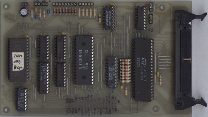
Euro-ZX81 CPU
Board V2 Component Side
|
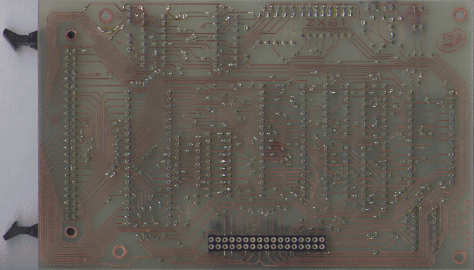
Euro-ZX81 CPU
Board V2 Solder Side
|

|

|
|
Euro-ZX81 Video
Board V3 Component Side
|
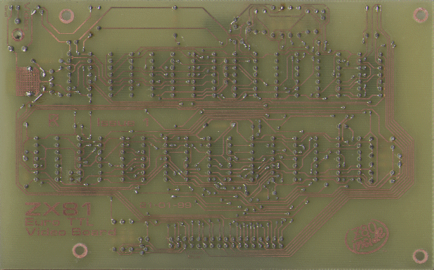
Euro-ZX81 Video
Board V3 Solder Side
|

|

|
|
Euro-ZX81 Boards
Assembled Side View
|
Male-Male precision
Connector strip
|
On this picture it is (hopefully) clearly
visible what I mean by a solid assembly in which the connections are reliable
because both PCBs are fastened into a solid assembly. On the right is a
picture of the male-male precision connector strip.
Expansion Devices
Pictures

|

|
|
ZX Euro Buffer/Poke
Board Component Side
|
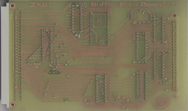
ZX Euro Buffer/Poke
Board Solder Side
|
I designed this ZX Euro Buffer/Poke PCB from
the original ZX-Team schematics and some email assistance from Kai Fischer(ZX-Team).
I already had a ZX-Team original Poke
Board, but needed a Signal buffer as well, so decided to integrate both
functions in this PCB to save space in the 19" rack. The flatcable connector
connects it to the Euro-ZX81 and the VG64 connector plugs directly into
the backplane PCB.

|

|
|
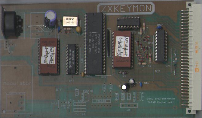
ZX AT Keyboard
Interface
|
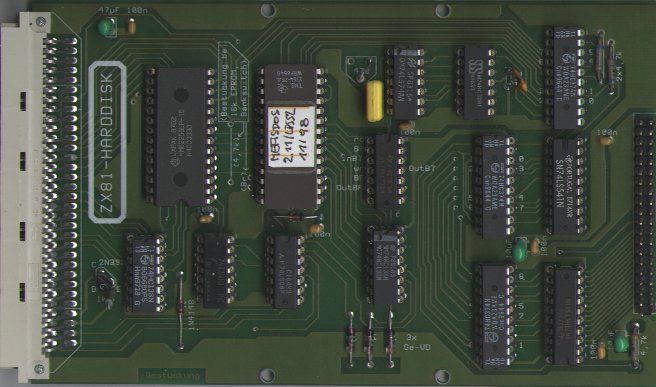
ZX Harddisk
Controller
|
These two pictures are both of ZX-Team original
PCBs that I use in my 19" assembly. The Harddisk Controller was built by
Kai Fischer since the specific configuration with the harddisk was a bit
tricky. The parameters are programmed into the EPROM which also contains
the MEFISDOS custom DOS developed by the German ZX-Team's Kai Fischer and
Joachim Merkl. I built the AT keyboard controller myself with the EPROMs,
RAM and 8049 microcontroller that I got from Kai Fischer together with
the PCBs.

|

|
|
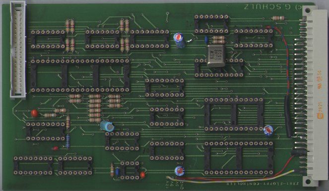
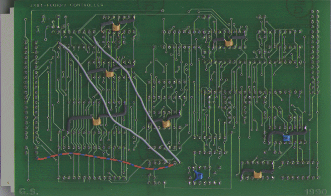
ZX Floppy Disk
Controller Component Side
|
ZX Floppy Disk
Controller Solder Side
|
This is the original ZX-Team Floppy Disk Controller,
a PCB design by G.Schultz dated 1990 according to the PCB's writing. I
built this PCB first to see how the Floppy interface operates. It was a
bit tricky to get this to work, as I found out it was related to the IC
types I used for the signal buffers on the Buffer/Poke Board. After some
experimenting with IC replacements on both the Buffer/Poke PCB and the
Floppy Controller PCB I got the entire system to work with a very high
reliability and perfect consistancy of stored and reloaded data. The wires
that are soldered onto the board are necessary because this original design
is of a period before the 19" assembly was used by the German ZX-team.
With only these few changes it can now simply be inserted into the 19"
rack.

|

|
|
ZX Floppy Disk
Controller Component Side
|
ZX Floppy Disk
Controller Solder Side
|
This board is my own PCB design made from
the original schematics of the ZX-Team Floppy Disk Controller. Basically
I did this design because I didn't like the loose wires that were necessary
to be added to the original Floppy Controller. (even though I still needed
to solder in a short wire on my own design prototype since this connection
was not in the original schematic. I also added a capacitor to stabilize
the Floppycontroller IC. These two small additions are now implemented
in my latest PCB design files.) An additional advantage of this board is
the fact that it's a single sided PCB design which is easier to build at
home.
19" Assembly Pictures

|

|
|
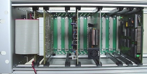
Front side photo
of 19" Assembly
|
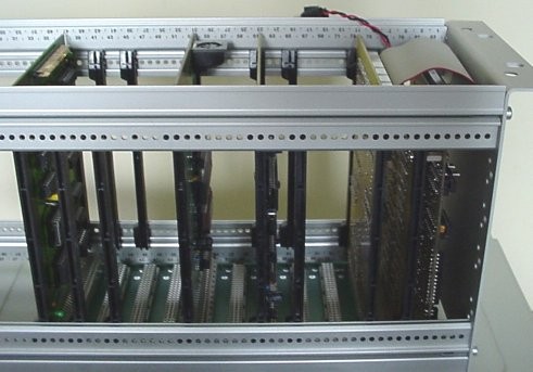
Top side photo
of 19" Assembly
|
From left to right (in left photo) - Euro-ZX81,
Buffer Poke Board, Floppy Disk Controller, AT keyboard Controller, Harddisk
Controller.

|

|
|
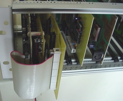
Close up 1 of
Euro-ZX81 and Buffer/Poke Board
|
Close-up 2 of
Euro-ZX81 and Buffer/Poke Board
|
Here you can see the flatcable connection
between the Euro-ZX81 and the Buffer/Poke VBoard.

|
|
Close Up of
jumpers made from precision connector pins
|
For some tips for making these, see the FAQ.
Some Further ZX81
Reading
To read more about the technical details
of the Euro-ZX81, proceed to the Euro-ZX81
Page.(See Horizontal Navigation bars)
With questions
I can be contacted by email
This
homepage is best viewed with Netscape.
Last update 27-03-2000 |