


![]()
![]()
![]()
![]()
![]()
![]()
Coherent
Optical Signal Detection
|
Document
Title |
Optical
Vector Demodulation |
|
Revision
Number |
|
|
Revision
Date |
|
|
Table
Of Contents
Coherent
Optical Signal Detection
Coherent
Detection For High Capacity Optical Networks
Unbalanced Coherent Detector Configuration
Single Balanced Optical Detector Using Optical Hybrids
Optical Vector Demodulation Using Optical Hybrids And Balanced Optical
Detectors
Physical
Implementation Details For The Optical Vector Demodulator
High
data capacity fiber optical networks typically combine single laser diode
transmitters combined with PIN diode detectors. Relatively simple binary on/off
switching is typical; some precautions are made to prevent complete extinction
of the transmitting laser diode but the basic configuration is relatively
simple.
The
configuration has 6 basic signal processing components
| Data
To Laser Diode Interface Driver | |
| Modulated
Transmit Laser Diode | |
| Fiber
Optic Cable Connection | |
| PIN
Photo Detector Diode | |
| Trans
Impedance Amplifier (TIA) | |
| Threshold
Detection Comparator |
Input
binary data is converted to a controlled current drive suitable for the laser
diode transmitter. This provides a controlled “high = 1” laser diode drive
current and an equally controlled “low = 0” laser drive current. A minimum
“off” current is maintained to improve switching times from an “off”
state to an “on state”. The resulting optical data stream is coupled to a
fiber optic cable and presented to a PIN Photo Detector diode that produces a
small analog output waveform corresponding to the data stream. A Trans-Impedance
Amplifier (TIA) converts this current waveform to an analog voltage waveform
whilst providing a low impedance termination required for fast response times.
Finally a Threshold Detection Comparator (TDC) decides a binary “1” or
“0” state from a potentially indeterminate input waveform.
Whilst
the standard approach is simple, it can still achieve data rates up to 10 GB/s
with standard optical transceiver modules. However it suffers from several
disadvantages
| Transmission
over long fiber optic cable can exhibit significant energy loss and weak
signal reception can be impaired due when the Signal To Noise Ratio (SNR)
falls below a critical threshold | |
| The
need to keep the laser diode “running” when “completely off” robs
the available SNR budget to some degree and the term “extinction ratio”,
in dB is used to indicate the degree of this available SNR impairment | |
| The
optical components have finite “BW” and the use of simple binary data
limits the data capacity to 1 Bit/Hz. In contrast, a coherent data scheme
based on Quadrature Amplitude Modulation (QAM) would provide 2 Bits/Hz or
greater data capacity. | |
| Over
long haul networks, the frequency dispersion effects of the fiber cable may
become significant and cause Inter Symbol Interference (ISI). Although some
equalization may be possible for the semiconductor components, the fiber
cable can only be equalized in a global average or “envelope” sense;
optical wavelength equalization in a vector sense is not possible. |
Some efforts have been made to increase data carrying capacity for fiber
optic networks using polarization diversity. This approach uses vertical
polarization for one channel and horizontal polarization for a secondary
channel. This dual channel configuration allows a form of vector signal
construction that provides opportunity for QPSK – QAM signal constructions
with associated improvements in Bits/Hz data throughput. For example, the use of
two independent channels automatically allows the channel capacity to double
over that of a single channel.
Although praiseworthy, this approach does not solve SNR issues, nor does
it facilitate vector equalization potentially required for long fiber cable
networks.
This document describes an alternative approach that might solve some of
these residual problems and therefore maximize the data capacity potential of
existing fiber cable networks. Although the cost of fiber cable is extremely
low, once a network is implemented, adding additional fibers can be cost
prohibitive. As we often find, user data capacity demands always exceed initial
estimates however well planned. Therefore it is in our best interests to have
secondary “back up” plans to better utilize data capacity of optical cable
networks already laid down.
Coherent
detection is used for measurements on weak optical signals. In this approach a
Local Oscillator (LO) is added to the incoming optical signal and non-linear
transfer characteristics inherent in a Photo Detection Device (e.g. a PIN photo
diode) produce a low relatively frequency base-band output signal.
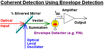
A
coherent local oscillator (laser) is used to heterodyne an optical input signal
down to a lower, more manageable baseband Intermediate Frequency (IF). This
configuration is typically used for weak optical signal detection but this
article will show how it can be modified to provide high data capacity transport
networks. A coherent, phase locked local oscillator (LO) is assumed.
The
frequency conversion different is subtly different from that used in
conventional RF signal processing. The input and LO optical waves are added as
complex exponentials prior to the photo detector. This component merely follows
the envelope variations resulting from the summation;
 …(1)
…(1)
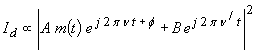
After
some trigonometric expansion we find the photo detector output current becomes
![]() …(2)
…(2)
We see
the emergence of a constant DC term, a frequency difference term n
- n/
and a relative phase term f.
We also see that the output current is proportional to the incoming optical
signal amplitude and the LO amplitude. This second proportionality shows the
potential for detector gain based on the addition of LO energy.
The
advantages of this heterodyne approach includes
| Optical
Amplification – the local oscillator adds energy that increases the
detector output signal level. This amplification reduces noise figure
demands on subsequent electronic processing. | |
| DC
Offset Removal – If the LO frequency is offset from the optical input
frequency, an AC beat frequency will be produced. This baseband signal can
then be amplified without a masking and potentially variable background DC
term | |
| Low
frequency noise sources arising from mechanical vibrations, 1/f
semiconductor noise etc is avoided. The baseband frequency can be placed
well above these spectral components. |
These
features make the heterodyne approach seem attractive for weak signal detection.
But how can it be used to solve the higher capacity problem?
The
solution to capacity enhancement is not based on an offset baseband IF approach
(essentially narrow band and low capacity) but instead combines the advantages
of heterodyne-based optical amplification with balanced optical detector design.
Further, the use of optical hybrids are proposed; in the radio frequency analog
these hybrids provide signal splitting and combining functions with varying
degrees of amplitude and phase distribution.

Two
identical photo detectors are used to produce matched baseband output signals.
The difference between each is taken to produce a combined output signal
centered at DC = 0 V.
The
optical LO is provided to each photo detector with equal amplitude and phase.
The Optical signal input is however presented with a 180 degree phase reversal.
An optical hybrid is used to produce this (wavelength independent) phase offset.
This
configuration provides an electronically amplified DC centered baseband output
that can produce positive and negative signal excursions. The effect of LO
amplitude variations (amplitude drift, amplitude perturbation noise) is
cancelled. Further the advantages of optical amplification is provided due to
the energy supplied from the LO source. Finally, the need for a frequency offset
is avoided, so that the maximum available photo-detector bandwidth is available.
This
single balanced optical detector provides a core component that will be used to
construct an optical Vector Demodulation component. It possesses the following
favorable characteristics
| DC
Offset errors are cancelled so that accurate optical conversion direct to DC
is available | |
| LO
Amplitude Noise is cancelled | |
| Full
photo-detector bandwidth is preserved | |
| Optical
amplification is available due to energy provided from the optical LO source |
The
previous heterodyne offset method solves the DC offset problem by producing a
band-pass baseband signal. However the cost of this solution is severely
constrained bandwidth capability. The single balanced optical detector
fundamentally solves the DC offset problem through balancing. Further, a
secondary “dark diode” is not simply used to provide a DC offset reference;
significant is the use of a second photo detector equally employed for Optical
to baseband signal conversion.
The use
of balanced mixers in vector demodulation devices is fundamental; extrapolating
the same concept to optical wavelengths appears relatively straightforward. We
require an additional optical hybrid component designed to produce dual outputs
with a 90 degree phase offset. This can be placed in either the optical or LO
paths, but the LO path implementation may provide a better practical
realization.
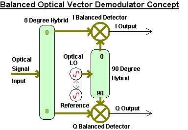
This new
configuration represents an optical analog of conventional analog IQ vector
demodulators. The independent I + j Q output, centered at DC, contain all the
complex signal information contained in the Optical input signal. In contrast to
a single detector, the IQ output contains independent spectral information above
and below the LO wavelength (frequency). Consequently, exact frequency
equalization for long, wavelength dispersive optical cables is possible.
In
summary, this optical vector signal demodulation component provides the
following key advantages over conventional approaches
| DC
Baseband I and Q Offsets are fundamentally cancelled | |
| LO
Amplitude Perturbation noise is cancelled, improving baseband SNR | |
| Photo
detector bandwidth is not “robbed” compared to frequency offset
approaches; therefore maximum possible photo-detector bandwidth and
therefore data rates are available | |
| Although
narrow bandwidth vector detection is provided (low pass filtering applied to
I and Q channels), the key advantage lays in efficient, complex signal
demodulation such as QPSK and high order QAM that provide high Bits/Hz
communication opportunity | |
| Optical
amplification, provided from LO energy is also provided, facilitating the
design of optical communication channels with optimal SNR performance |
Aside:
The LO is assumed to be coherent with the
incoming optical signal. As shown, an external, frequency stable reference is
assumed to be available for “phase locking” the laser LO source. In
principle, this reference can also be propagated along the fiber cable as a
“pilot tone” added to the optical signal. Conventional approaches used to
impart a narrow band optical carrier on an otherwise unusable part of the fiber
cable’s wavelength “windows” are readily available; for example a 10 MHz
reference could be used to directly modulate a secondary LED source that
occupies some other portion of the optical spectrum and detected at the
receiving end, therefore reconstructing the original 10 MHz reference.
Since this reference is continuous, narrow band
detection is appropriate. This can use conventional LC band pass filtering
followed by Phase Locked Loop (PLL) noise cleanup. The technical difficulties
associated with this approach are minimal; also the solution is extremely cost
effective and would probably cost less than $10 per system.
However this overhead, albeit small, is probably
not required for high-speed data. As is typical in high capacity QAM systems,
symbol package synchronization is used to remove frequency-offset errors. In
this strategy, short symbol packages are sent, during each symbol interval,
frequency offset errors correspond to relatively small phase offset errors that
can be made negligible. Standard carrier phase tracking algorithms operate as
background tasks and ensure coherent signal recovery even though LO and incoming
RF signals are not coherent. This approach becomes increasingly attractive as
bandwidth increases and symbol and package time length decreases.
We will
assume modern high performance electronic and optical signal processing
components are available operating at 10 GB/s. If moderate components are
substitute, the same capacity gains will be achieved (by scaling), but the main
thrust of this approach is to extract maximum data capacity from existing
networks, so the employment of lower performance processing elements would seem
to be counter productive to this goal.
The
simplest vector constellation is QPSK. This immediately provides 2 Bits/s
performance gain. We can therefore predict the improved data capacity to double
the previous 10 GB/s limitation to 20 GB/s.
One
variation on QPSK is DQPSK. This “differential” constellation offers
significant relaxation on frequency and phase stability as each symbol is
effectively measured against its predecessor. The penalty for this
“robustness” is 3 dB degradation in ultimate SNR; however this deficit may
be quite survivable given the high potential already afforded from LO enhanced
optical amplification.
It would
be desirable to consider higher order constellations however. For example, QAM16
would provide 4 Bits/Hz and predicts a data throughput potential of 80GB/z. Even
larger constellations, such as QAM256 provide 8 Bits/Hz and an associated
throughput potential of 160 GB/s.
Still
higher level constellations may benefit from channel equalization, but as
mentioned previously, the vector IQ demodulator allows full optical channel
equalization i.e. both sides of the optical spectrum can be treated
independently. This is not possible for a single photo detector approach, nor is
it available for polarization diversity approaches.
A
further serendipitous outcome is that OFDM modulation formats can also be
processed. These formats have fundamental “built in” immunity from
dispersive channel aberrations based on their multiple sub carrier approach.
Each sub carrier could, in principle, carry QAM256 payloads and so the full
fiber link capability can be exploited.
A
demonstration optical vector demodulator can be fabricated with standard “off
the shelf” components. Whilst this would demonstrate “proof in principle”,
an Integrated Circuit (IC) implementation would be required for a practical
implementation.
The IC
implementation is preferred as this ensures maximum possible component matching.
The degree of DC offset cancellation, for example, would greatly exceed that
possible from discrete components. Further, the long optical path lengths
required with relatively large physical processing components would be difficult
to maintain with good phase integrity. On an IC scale of dimension, these
optical paths would be wavelength comparable and therefore fortuitously easier
to manage.
The
resulting IC could be mounted in a standard carrier package with separate
optical LO and optical signal inputs. Although an internal laser diode could be
incorporated, at least in principle, the thermal problems associated with its
operation might prove problematic. Further, the silicon fabrication technologies
might not be compatible with those required for other signal processing
components such as photodiodes and transistors required for high speed
electronic processing. For these, the use of Silicon-Germanium (SiGe) is
probable, whilst laser diodes might be fabricated on a GaAs process.

As
shown, a number of optical hybrids are needed for photonic distribution.
Specifically we need the following
| 180
Degree Phase Shift Hybrid | |
| 90
Degree Phase Shift Hybrid | |
| 0
Degree Phase Shift Hybrid |
The
180-degree hybrid should ideally introduce its phase inversion as a fundamental
property, as opposed to merely adding a propagation time delay – this approach
could be overly wavelength dependent and a “broad band” approach would be
preferable.
The
easiest way to generate is to use reflection. A wave undergoes a 180-degree
phase inversion on reflection. The reference throughput path would be equivalent
to zero degrees.
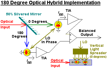
This
diagram shows the geometric configuration required to realize an equal optical
path 180 degree hybrid and a constant phase LO illumination hybrid. The hybrid
loss will be 3dB for the optical input (50% “silvered mirror”) but the 0
degree LO hybrid can afford to be far less efficient. Additional LO power can be
provided to overcome LO loss but optical input loss cannot be readily
compensated.
The
180-degree hybrid will be implemented as a planar structure on the silicon IC
substrate. The “overhead lighting” from the “Vertical Light Spreader”
will provide equal illumination for each photo diode with equal optical path
length and hence equal wavelength independent phase. The key advantage for this
single balanced optical mixer is theoretical wavelength independence. The DC
balance remains matched despite LO frequency and the phase and amplitude
accuracy of the 180 degree input phase shift hybrid is equally wavelength
independent.
The
electronic baseband output paths will also be of equal length. The Trans
Impedance Amplifiers (TIA) will terminate each photo diode in close proximity
and an ultra fast difference amplifier will provide the final output (In
practice this will be rotated 45 degrees for improved symmetry).

The
optical input signal is split equally upwards and downwards in this diagram
using two 45-degree mirrors presenting a sharp intersecting wedge. The two split
waves have equal phase and amplitude and travel towards each balanced mixer.
Additional mirrors are placed symmetrically to ensure correct orientation and
equal path length.
The LO
input also uses this approach but introduces an additional time delay equivalent
to 90 degrees phase shift at the center operating wavelength. This distribution
can be implemented on a plane just above (or below) the dual diode balanced
mixers and then distributed vertically to the PIN diode detectors. Unlike the
other hybrids, the phase distribution accuracy of the 90-degree version is
directly affected by wavelength. This may not be problematic however, as phase
skew errors can be removed at IQ baseband (for example, cross coupling a portion
of I into Q and vice versa can introduce an opposite phase skew error).
Summary
A wide
band optical vector demodulator appears feasible; although implementation is
possible with discrete components, and a prototype “proof in principle”
intermediate step would be valuable, a practical usable implementation would
best be fabricated on a silicon substrate using conventional die processing
methods. The speed advantages afforded from SiGe technologies have been well
exploited in recent times and almost every new high frequency components using
Bipolar transistors adopts this fabrication. Whilst CMOS is not excluded,
certain components, e.g. PIN photodiodes have to use structures similar to
bipolar junction devices.
The
laser LO source is probably best left as an external, technology specialized
component. This may be phase locked to an accurate frequency reference or, in
the wide band data cases, might well be adequately left to “free run”.
The use
of equivalent matched photodiode pairs provides automatic DC balance and avoids
the need for offset heterodyne architectures. Therefore narrow band, high
sensitivity applications are enabled as readily as wide band, high data capacity
complex modulation formats.
![]()
![]()
![]()
![]()
© Ian Scott 2009
