This article introduces
the most humble of the semiconductor devices – the Diode. Its
predecessor was the Thermionic vacuum tube diode, widely used for
high voltage AC to DC power supply rectification and small signal
radio frequency signal detection, typically required in early
valve AM and FM broadcast radios. The solid state diode was seen
in those early days as a panacea for energy wasteful “heated
cathode emitters”, and although the introduction of inert gases
into “mercury vapour rectifiers”, offset, to some extent, the
high voltage drop losses of vacuum tube diodes, the march for
solid state continued. This article parades the victory of the
semiconductor diode, which today surmounts most, if not all posts
once held by the vacuum or its gas filled cousins. Its many
variants are introduced, and their new applications and associated
electronic behaviours are described, especially for RF usage.
|
|
Document
Summary of Contents
|
|
CONFIDENTIAL
This document is not to be
copied, transferred electronically or otherwise without prior
written consent from the Author.
DISTRIBUTION
This document may only
be shown to others with the Author’s prior consent.
|
|
1 Table
of Contents........................................................................
2
2
Preface To Semiconductor Diodes
 ...............................................
4
...............................................
4
2.1
General Comments On The Subject Of Semiconductor Diodes.....................................................
4
2.2
What This Document Contains.......................................................................................................................
4
3
A Short History Of Semiconductor Diode Devices...............................
6
3.1
A Perspective On Semiconductor Technology Progress...................................................................
6
3.2
Recollections Of Much Earlier Semiconductor Devices..................................................................
6
3.2.1
A Short Diversion Into “Coherer” Radio Telephony Receiver Technology.................................
6
3.2.2
The “Copper Oxide Rectifier” For Low Cost Battery Charger Application................................
7
3.2.3
The “Selenium Rectifier” For High Voltage High Efficiency AC to DC
Rectification
 and
Small Signal Audio Limiter Applications............................................................................................................................................
8
and
Small Signal Audio Limiter Applications............................................................................................................................................
8
3.2.4
The Point Contact Germanium Diode Designed For Small Signal Radio
Frequency (AM) Detection
 9
9
4
Modern Semiconductor Junction Diode Construction And Applications
10
4.1
General Semiconductor Junction Diode Types...................................................................................
10
4.1.1
Germanium Junction Diode Construction...............................................................................................
10
4.1.2
Silicon Junction Diode Types....................................................................................................................
10
4.2
Silicon Diodes For Radio Frequency Applications..........................................................................
14
4.2.1
Schottky Diode Construction.....................................................................................................................
14
4.2.2
Varicap Diode Construction........................................................................................................................
14
4.2.3
PIN Diode Construction...............................................................................................................................
15
4.2.4
Zener and Avalanche Diode Construction.............................................................................................
15
4.2.5
Photodiode Construction..............................................................................................................................
15
4.2.6
Solar Cell Construction................................................................................................................................
15
4.2.7
Light Emitting Diode Construction............................................................................................................
15
5
Electrical Properties Of Semiconductor Junction Diodes...................
17
5.1
Description Of Terminology..........................................................................................................................
17
5.2
Semiconductor Junction Diode Static DC Characteristics.......................................................
17
5.2.1
Semiconductor Junction Diode Forward and Reverse DC Characteristics..............................
17
5.2.2
DC Imperfections In Real Junction Diodes.........................................................................................
19
5.3
PN Junction Diode Reverse Breakdown Modes...................................................................................
20
5.3.1
Avalanche Diode Voltage Regulation......................................................................................................
20
5.3.2
Zener Diode Voltage Regulation...............................................................................................................
21
5.4
Junction Diode Temperature Dependence...............................................................................................
21
5.5
The Dynamic Characteristics Of Semiconductor Junction Diodes.......................................
22
5.5.1
Dynamic Impedance Of Forward Biased Diode.................................................................................
22
5.6
The RF Characteristics Of PN Junction Diodes.................................................................................
25
5.6.1
Forward Biased Capacitance.....................................................................................................................
25
5.6.1.1
Diode Series Resistance.............................................................................................................................
25
Composite
Junction Diode Model..............................................................................................................................
25
5.6.2
PN Junction Diode Reverse Biased Capacitance...............................................................................
26
6
Appendix....................................................................................
27
6.1
Transistor reference.........................................................................................................................................
27
6.1.1
The Point Contact Germanium Transistor.............................................................................................
27
6.2
Subject 2....................................................................................................................................................................
28
This
document opens with a short history on diode applications in general, beginning
with the primitive “almost a diode” Coherer detector used for Morse Code
reception and rusty copper oxide AC-DC rectifiers. Better semiconductor
materials such as Selenium were soon discovered, leading to higher voltage AC to
DC power rectification and low frequency audio signal application. RF signal
applications began around the time of the “point contact signal diode”,
which had sufficiently low capacitance to allow signal detection up to several
hundred MHz. Germanium gained an early status due to its ease of manufacture and
today Silicon reigns. Much interest is also shown in Carbon (diamond) and
compound semiconductor materials such as Gallium Arsenide, Silicon Germanium,
Indium Gallium Phosphorous, etc.
Various
Diode families are then described in applications that go far beyond those
simple rectification tasks they first gained footholds in. Today various diode
versions are used for voltage regulation
 , dual polarity transient energy suppression
 and electronically tuned filters
 found in AM and FM car radios and
TV sets. They are used in microwave applications that require electronic control
of signal amplitude and also provide protection against high amplitude signal
microwave signal pulses. Photo detection diodes
found in AM and FM car radios and
TV sets. They are used in microwave applications that require electronic control
of signal amplitude and also provide protection against high amplitude signal
microwave signal pulses. Photo detection diodes
 are available for infrared energy
and light, and can even be used for optical wavelength conversion when combined
with a Laser Local Oscillator source. Optically “pure” Laser Light Emitting
Diodes (LED’s)
are available for infrared energy
and light, and can even be used for optical wavelength conversion when combined
with a Laser Local Oscillator source. Optically “pure” Laser Light Emitting
Diodes (LED’s)
 are used in every CD player and
their less optically coherent counterparts are used as visual indicators on
almost every electrical appliance. “White LED’s” are even available now to
replace Edison’s incandescent light bulb
are used in every CD player and
their less optically coherent counterparts are used as visual indicators on
almost every electrical appliance. “White LED’s” are even available now to
replace Edison’s incandescent light bulb
 used for ambient lighting. Even
“Solar Cells” used to directly convert the sun’s energy to electricity are
made of diodes. In some ways, Semiconductor Diodes have filled more application
fields than any other electronic component. Perhaps that’s not bad for
something that begun from accidental contacts between rusting metal surfaces and
early broadcast “AM” radio receivers made from fine wire probes searching
for trace selenium deposits on common lumps of coal
used for ambient lighting. Even
“Solar Cells” used to directly convert the sun’s energy to electricity are
made of diodes. In some ways, Semiconductor Diodes have filled more application
fields than any other electronic component. Perhaps that’s not bad for
something that begun from accidental contacts between rusting metal surfaces and
early broadcast “AM” radio receivers made from fine wire probes searching
for trace selenium deposits on common lumps of coal

 .
.
This document describes the construction
and characteristics of the following diode classes.
- Early
Semiconductor Diode (or Diode Like) Devices
-
The
“Coherer” used to receive slow speed Morse code radio messages
-
The
Copper Oxide “Battery Charger” Rectifier
-
The
Higher Voltage “Selenium” Rectifier
-
The
Small Signal Audio Diode, Also Based on Selenium
-
The
First RF Component, The Germanium Point Contact Signal Diode
- More
Recent Semiconductor Diodes
-
The
Germanium PN-Junction Diode Used For Switching
-
The
Tunnel Diode (Or Esaki Diode after its Inventor Leo Esaki)
- Modern
Semiconductor P-N and Related Junction Diodes
-
The
Silicon Diode Used For Switching
-
The
Schottky Diode Used For High Speed Rectification and Microwave Applications
-
Silicon
and Gallium Arsenide Variable Capacitance “Varactor” or “Varicap” Diodes
Used For Electronic Tuning in Filters and Oscillators
-
Silicon
Zener and Avalanche Diodes Used For Voltage Regulation and Clamping
-
Silicon
P-I-N Diodes Use For Variable Attenuation and Band Switching
-
Photo-Detector
Diodes
-
Solar
Cell Diodes
-
Light
Emitting Diodes (LED’s and also LASER Diode)
The electrical characteristics for the
following topics are also described in further detail.
- Reverse
Biased Varicap Diode C-V Characteristics
- PIN
Diode Carrier Lifetime
 and its Relationship to
Intermodulation Distortion
and its Relationship to
Intermodulation Distortion
- Forward
Biased PN-Junction Diode “Charge Based” Capacitance
An appendix containing various MATHCAD
Demonstrating files is also included in this document.
The semiconductor age has revolutionised
electronics with miniaturised circuits performing convenient, advanced signal
processing functions. Semiconductor devices are used for power electronics,
audio amplification, radio frequency amplification, optical processing and
digital computations.
Prior to this we lived in a land of
wires, relays, twine and sealing wax. Even the emergence of De Forest’s vacuum
tube
 belonged to an era of hand-connected components mounted on bent, drilled and
machined metal chassis bolted into equally hand crafted wooded cabinets.
Although nostalgic to some, individual production of such expensive items was
never an ambition of the industrial revolution. Mass production, based on
repetitive tasks, each being a sub component of the whole, was the enviable
position to be attained. Towards this end we saw the use of PCB substrates
supporting leaded components and socket held valves, each searing their
surroundings with heat for the purpose of relatively simple signal processing.
belonged to an era of hand-connected components mounted on bent, drilled and
machined metal chassis bolted into equally hand crafted wooded cabinets.
Although nostalgic to some, individual production of such expensive items was
never an ambition of the industrial revolution. Mass production, based on
repetitive tasks, each being a sub component of the whole, was the enviable
position to be attained. Towards this end we saw the use of PCB substrates
supporting leaded components and socket held valves, each searing their
surroundings with heat for the purpose of relatively simple signal processing.
The semiconductor promise was one of
reduced size and heat, both of which beckoned more complex signal processing
tasks to be performed. As the number of semiconductor components increased,
reliability issues became increasingly important. Anecdotal stories of house
sized computers built with vacuum tubes serviced by teams of technicians
repairing defects every few hours are easily found. The translation to
transistors, at first based on at least one occasion by the “point contact”
germanium transistor improved this situation considerably. The grand centre
stage show belongs to the invention of the integrated circuit, for which the
photographic process used for device definition and interconnection has become
tuned to a fine art. Resolutions available today parade themselves at a fraction
of the wavelength of light used for creating the lithographic screens used for
device fabrication. Complexity, Heat and Reliability issues are now replaced by
those associated with Software Reliability.
The ocean going ships of the time had
crude communication technologies, involving the use of semaphore for
transferring simple messages, or the use of loud fog-horn calls to at least
state occupancy in fog laden seas. In isolation, Nikola Tesla had been
experimenting with coils that made high voltage discharges, with a dream in mind
of sending electronic power between the continents of the world, huddled between
the blankets of transmission line effects between the planets surface and its
ionosphere. Equally remote, Marconi also played with sparks, sending them from
the ends of one wire loop into the gap of another. In some “lair of
Frankenstein” way both experiments sparked forth the birth of a new
communications industry. However, the distances electric fields could cross only
existed within the confines of a small experimenter’s room. For sea-to-land
communications, something more sensitive than the electrical breakdown of air
was needed. However, on the positive side (no pun intended), ocean going ships
with their massive diesel generators had almost unlimited power to send.
I guess some people thought about this
and reasoned that the distance of the receiving spark gap was the other part of
the problem. (Perhaps there are transactions on this subject?) How could the gap
be made smaller so that the tiny sparks could fly across and make their mark?
One idea was to fill a glass tube with
rusting iron filings. Electrodes were attached to each end, and a source of
voltage was applied through headphones. Normally the iron filings would make
poor contact, but when a RF pulse came along some of the filings would arc and
short, allowing a DC current to pass.
The
“coherer” was actually quite sensitive at detecting RF signals
but it could only do it once. Once fired, it continued to conduct,
making it a “1 bit detector”. The operator had to tap it loose
after each headphone click and it would be ready for action again.
More advanced arrangements attempted to automate this procedure,
but at least slow reception of Morse-code clicks could be
received.
|
|
Morse Code was the coherer’s domain
and it was firmly thought to be there to stay. Or so it seemed – until De
Forest’s vacuum diode came along, and the coherer’s brief life was over.
The semiconductor based rectification
properties of various metal oxides had been observed long before the invention
of the vacuum tube diode. Of these, rectifiers formed from copper disks
sandwiched between iron ones were popular. Their main application was for low
frequency AC to DC conversion, such as that required for car battery charging.
However these assemblies had a relatively low reverse breakdown voltage and
several disks were needed to rectify AC voltages even as low as 6 V AC. The
unfortunate consequence was relatively inefficient AC to DC conversion
efficiency due to the cumulative forward voltage drop of each individual
rectifying disk. In addition, the screwed down washer-by-washer construction was
not suited to automated construction, although the cost of each iron washer and
insulating disc was low.

Selenium rectifiers followed copper
oxide devices, and were best suited to lower current, high voltage rectification
such as required by valve high tension DC supplies up to 250 V DC. They were
also based on a stacked construction, but thin rectangular slabs were used
instead of washers. Some small signal “selenium diodes” were also produced,
used for audio clipping applications such as car AM radio impulse noise blanker
applications.
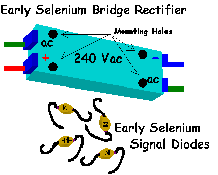
Selenium rectifiers survived for some
time as high voltage rectifiers in valve based AM radios for medium and short
wave broadcast radios, based on their relatively small size compared to a
dedicated rectifier tube, absence of a heated cathode and relatively low cost.
Germanium rectifiers were possible at the time, based on alloy junction
construction, but had high leakage current, especially with the temperatures
expected in a typical valve radio. The high voltages encountered were also a
major stumbling block, as the several hundreds of volts required in vacuum tube
radios was far high than the 30 V average best ratings of Germanium. Even if
these obstacles were overcome, device failure due to “thermal runaway” was
probable. Leakage current made worse by increasing temperature lead to
additional heating that further exacerbated the leakage problem. Device
destruction soon followed. Given this, even stacked series combinations of
Germanium diodes were never feasible.
Consequently, Selenium rectifiers lasted
right up to the advent of Silicon junction diodes, coinciding about the time of
the “planar” photolithographic process. These new improved Silicon devices
sprang into the spotlight immediately, armed with forward voltage drops less
than 1 Volt and reverse blocking capability exceeding 400 Volts, even to 100
Volts with minor tweaks. Overnight, once again, old technology was tossed out
from its comfortable home in favour of the new, and the selenium rectifier’s
days of notoriety were over even faster than it ousted the copper oxide
rectifier that previously overthrew the vacuum valve.
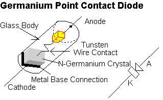
Point contact diodes can be formed by
pressure contact between a metal electrode and a semi-conductive substance. The
earliest signal detection applications might have involved “Paul Hogan” and
his captured men fingering a piece of coal at “Stalag 9” in a TV episode of
“Hogan’s Hero’s”, or so when young we might have believed. Such episodes
often portrayed a captured soldier straining to hear an allied radio broadcast
on a pair of army issue magnetic headphones, right under the nose of the
imprisoning “Colonel Clink”. A lump of coal, in this case poised against the
spring of a wire whisker, would have contained traces of selenium and containing
carbon, was adequately conductive as a substrate. Hence the first “TV Radio
Diode!” bought AM (short-wave?) messages to the troops.
Commercial production of point contact
diodes began early, fuelled by the communication needs of WW1, but also because
they were easy to manufacture, and with profit, also their low self-capacitance
made them useful for Radar detection. The standard semiconductor was Germanium.
|
|
Germanium point contact
diodes were originally housed in metal containers and used for
microwave signal detection in early radar systems
 . For commercial
applications the sturdy metal housing was replaced with a lower
cost drawn glass cylinder. . For commercial
applications the sturdy metal housing was replaced with a lower
cost drawn glass cylinder.
Diodes preceded the
invention of the transistor but became used with them as a simple
AM detector in AM Broadcast transistor radios.
|
|
Germanium point contact diodes had
reverse leakage currents in the order of 1 uA, and a forward voltage drop around
0.2 V at currents less than 1 mA. They were well suited to RF signal detection
at frequencies up to several hundred MHz even in their commercial cylindrical
glass package, due to their low self-capacitance usually less than 0.5 pF.
The PN junction was formed from
impurities in the wire contact (Tungsten, etc) combining with the Germanium
crystal. This was often assisted by “forming”, a process whereby a short
electronic pulse was passed between the electrodes. This helped to establish a
secure and stable PN region.
Note:
In this way the Germanium point contact diode does not resemble a “Schottky”
diode, which is based on a direct metal to semiconductor junction. Although a
Germanium point contact diode may use a metal contact, this contact is used to
form a P-N junction immediately under its tip, and the metal wire contact then
becomes a simple connecting electrode.
The semiconductor age has revolutionised
electronics with miniaturised circuits performing convenient, advanced signal
processing functions. Semiconductor devices are used for power electronics,
audio amplification, radio frequency amplification, optical processing and
digital computations.
Prior to this we lived in a land of
wires, relays, twine and sealing wax. Even the emergence of De Forest’s vacuum
tube
 belonged to an era of hand-connected components mounted on bent, drilled and
machined metal chassis bolted into equally hand crafted wooded cabinets.
Although nostalgic to some, individual production of such expensive items was
never an ambition of the industrial revolution. Mass production, based on
repetitive tasks, each being a sub component of the whole, was the enviable
position to be attained. Towards this end we saw the use of PCB substrates
supporting leaded components and socket held valves, each searing their
surroundings with heat for the purpose of relatively simple signal processing.
belonged to an era of hand-connected components mounted on bent, drilled and
machined metal chassis bolted into equally hand crafted wooded cabinets.
Although nostalgic to some, individual production of such expensive items was
never an ambition of the industrial revolution. Mass production, based on
repetitive tasks, each being a sub component of the whole, was the enviable
position to be attained. Towards this end we saw the use of PCB substrates
supporting leaded components and socket held valves, each searing their
surroundings with heat for the purpose of relatively simple signal processing.
The semiconductor promise was one of
reduced size and heat, both of which beckoned more complex signal processing
tasks to be performed. As the number of semiconductor components increased,
reliability issues became increasingly important. Anecdotal stories of house
sized computers built with vacuum tubes serviced by teams of technicians
repairing defects every few hours are easily found. The translation to
transistors, at first based on at least one occasion by the “point contact”
germanium transistor improved this situation considerably. The grand centre
stage show belongs to the invention of the integrated circuit, for which the
photographic process used for device definition and interconnection has become
tuned to a fine art. Resolutions available today parade themselves at a fraction
of the wavelength of light used for creating the lithographic screens used for
device fabrication. Complexity, Heat and Reliability issues are now replaced by
those associated with Software Reliability.
The ocean going ships of the time had
crude communication technologies, involving the use of semaphore for
transferring simple messages, or the use of loud fog-horn calls to at least
state occupancy in fog laden seas. In isolation, Nikola Tesla had been
experimenting with coils that made high voltage discharges, with a dream in mind
of sending electronic power between the continents of the world, huddled between
the blankets of transmission line effects between the planets surface and its
ionosphere. Equally remote, Marconi also played with sparks, sending them from
the ends of one wire loop into the gap of another. In some “lair of
Frankenstein” way both experiments sparked forth the birth of a new
communications industry. However, the distances electric fields could cross only
existed within the confines of a small experimenter’s room. For sea-to-land
communications, something more sensitive than the electrical breakdown of air
was needed. However, on the positive side (no pun intended), ocean going ships
with their massive diesel generators had almost unlimited power to send.
I guess some people thought about this
and reasoned that the distance of the receiving spark gap was the other part of
the problem. (Perhaps there are transactions on this subject?) How could the gap
be made smaller so that the tiny sparks could fly across and make their mark?
One idea was to fill a glass tube with
rusting iron filings. Electrodes were attached to each end, and a source of
voltage was applied through headphones. Normally the iron filings would make
poor contact, but when a RF pulse came along some of the filings would arc and
short, allowing a DC current to pass.
The
“coherer” was actually quite sensitive at detecting RF signals
but it could only do it once. Once fired, it continued to conduct,
making it a “1 bit detector”. The operator had to tap it loose
after each headphone click and it would be ready for action again.
More advanced arrangements attempted to automate this procedure,
but at least slow reception of Morse-code clicks could be
received.
|
|
Morse Code was the coherer’s domain
and it was firmly thought to be there to stay. Or so it seemed – until De
Forest’s vacuum diode came along, and the coherer’s brief life was over.
The semiconductor based rectification
properties of various metal oxides had been observed long before the invention
of the vacuum tube diode. Of these, rectifiers formed from copper disks
sandwiched between iron ones were popular. Their main application was for low
frequency AC to DC conversion, such as that required for car battery charging.
However these assemblies had a relatively low reverse breakdown voltage and
several disks were needed to rectify AC voltages even as low as 6 V AC. The
unfortunate consequence was relatively inefficient AC to DC conversion
efficiency due to the cumulative forward voltage drop of each individual
rectifying disk. In addition, the screwed down washer-by-washer construction was
not suited to automated construction, although the cost of each iron washer and
insulating disc was low.
Selenium rectifiers followed copper
oxide devices, and were best suited to lower current, high voltage rectification
such as required by valve high tension DC supplies up to 250 V DC. They were
also based on a stacked construction, but thin rectangular slabs were used
instead of washers. Some small signal “selenium diodes” were also produced,
used for audio clipping applications such as car AM radio impulse noise blanker
applications.
Selenium rectifiers survived for some
time as high voltage rectifiers in valve based AM radios for medium and short
wave broadcast radios, based on their relatively small size compared to a
dedicated rectifier tube, absence of a heated cathode and relatively low cost.
Germanium rectifiers were possible at the time, based on alloy junction
construction, but had high leakage current, especially with the temperatures
expected in a typical valve radio. The high voltages encountered were also a
major stumbling block, as the several hundreds of volts required in vacuum tube
radios was far high than the 30 V average best ratings of Germanium. Even if
these obstacles were overcome, device failure due to “thermal runaway” was
probable. Leakage current made worse by increasing temperature lead to
additional heating that further exacerbated the leakage problem. Device
destruction soon followed. Given this, even stacked series combinations of
Germanium diodes were never feasible.
Consequently, Selenium rectifiers lasted
right up to the advent of Silicon junction diodes, coinciding about the time of
the “planar” photolithographic process. These new improved Silicon devices
sprang into the spotlight immediately, armed with forward voltage drops less
than 1 Volt and reverse blocking capability exceeding 400 Volts, even to 100
Volts with minor tweaks. Overnight, once again, old technology was tossed out
from its comfortable home in favour of the new, and the selenium rectifier’s
days of notoriety were over even faster than it ousted the copper oxide
rectifier that previously overthrew the vacuum valve.
Point contact diodes can be formed by
pressure contact between a metal electrode and a semi-conductive substance. The
earliest signal detection applications might have involved “Paul Hogan” and
his captured men fingering a piece of coal at “Stalag 9” in a TV episode of
“Hogan’s Hero’s”, or so when young we might have believed. Such episodes
often portrayed a captured soldier straining to hear an allied radio broadcast
on a pair of army issue magnetic headphones, right under the nose of the
imprisoning “Colonel Clink”. A lump of coal, in this case poised against the
spring of a wire whisker, would have contained traces of selenium and containing
carbon, was adequately conductive as a substrate. Hence the first “TV Radio
Diode!” bought AM (short-wave?) messages to the troops.
Commercial production of point contact
diodes began early, fuelled by the communication needs of WW1, but also because
they were easy to manufacture, and with profit, also their low self-capacitance
made them useful for Radar detection. The standard semiconductor was Germanium.
|
|
Germanium point contact
diodes were originally housed in metal containers and used for
microwave signal detection in early radar systems
 . For commercial
applications the sturdy metal housing was replaced with a lower
cost drawn glass cylinder. . For commercial
applications the sturdy metal housing was replaced with a lower
cost drawn glass cylinder.
Diodes preceded the
invention of the transistor but became used with them as a simple
AM detector in AM Broadcast transistor radios.
|
|

Germanium point contact diodes had
reverse leakage currents in the order of 1 uA, and a forward voltage drop around
0.2 V at currents less than 1 mA. They were well suited to RF signal detection
at frequencies up to several hundred MHz even in their commercial cylindrical
glass package, due to their low self-capacitance usually less than 0.5 pF.
The PN junction was formed from
impurities in the wire contact (Tungsten, etc) combining with the Germanium
crystal. This was often assisted by “forming”, a process whereby a short
electronic pulse was passed between the electrodes. This helped to establish a
secure and stable PN region.
Note:
In this way the Germanium point contact diode does not resemble a “Schottky”
diode, which is based on a direct metal to semiconductor junction. Although a
Germanium point contact diode may use a metal contact, this contact is used to
form a P-N junction immediately under its tip, and the metal wire contact then
becomes a simple connecting electrode.
Although the Germanium point contact
diode enjoyed great success as a small signal detection diode, it had a
relatively high series resistance that limited its ability to handle currents
beyond a few milli-amperes or to act as logic elements in semiconductor based
computers. The small area of contact was responsible. In addition, its
electrical characteristics were unpredictable, partly due to the mechanical
nature of its formulation, the imprecise nature of “forming” and also the
uncontrolled impurities that could be expected from one Germanium crystal to the
next.
The Germanium junction diode was born
from advances in the science of growing large, chemically pure crystals.
Further, the concept of “doping” a given crystal with impurities that could
result in an excess of electrons (Arsenic doping produces N - Type material) or
an excess of holes (Boron doping produces P- Type material) was in hand during
the second-world war. Chemical vapour deposition could then be used to create an
accurate PN junction on a single Germanium wafer, which could then be bonded to
or pressed against suitable wire electrodes.
|
|
Germanium junction diodes
intended for small signal switching applications were usually
based on the “point contact” construction using a small glass
envelope. However, these diodes had a doped + Type region which
the “whisker” contact made electrical connection with. These
diodes were often doped using Gold, resulting in lower series
resistance than would otherwise occur.
|
|
Germanium semiconductor junction diodes
reigned up to the 1970’s, used mainly in discrete semiconductor based computer
mainframe equipment. They formed simple AND gates and OR gate logic elements
that required a low forward voltage drop, fast switching and acceptably low
leakage. Once again, however, the tides were turning on yet another established
technology in favour of a newer breed. Silicon had long been envied for its high
temperature resilience, up to a predicted maximum of 200 C, compared to
Germanium that failed miserably at 90 C. Although plentiful (as Silicon-Oxide or
sand), purity was a serious barrier to Silicon’s commercial use. Small
molecular imperfections could render an otherwise viable PN-Diode structure
useless, resulting in unattractively low yields.
The Silicon Junction diode was placed
“centre stage” as soon as this crystal purity barrier was broken. These
diodes soon adopted the “planar” photographically processed substrate
method, and were initially housed in the same glass envelop as their Germanium
cousins. They offered a low cost, ultra low reverse leakage diode with excellent
RF and switching characteristics. They even replaced the familiar Germanium
point contact diode in AM radio detector circuits, especially when these also
switched to silicon planar transistors instead of slower, low gain and
temperature intolerant Germanium devices.
Today’s Silicon junction diodes are
constructed simply without te potentially unreliable wire contact
(“whiskerless diode”) and have changed very little from their introduction
around 1960. A planar lithographic process is used, and surface mount housing is
now standard unless high power dissipation is required.
The Silicon (Si) junction diode consists
of a N-Type substrate with a Diffused P-Type upper surface. Metal contacts are
made to each surface for electrical connection. Potential “Intrinsic”
semiconductors and their potential “Doping” elements can be seen as adjacent
columns in the following periodic table,
Truncated
Periodic Table
|
Period
|
III-A
3-A
|
IV-A
|
|
Advantages
of IVA Semiconductor
|
Use
|
|
Row
|
|
2
|
B
Boron
|
C
Carbon
|
N
Nitrogen
|
Very-High Temperature
|
Future
|
|
3
|
|
Si
Silicon
|
P
Phosphorous
|
High Temperature, Cheap
|
Common
|
|
4
|
Ga
Gallium
|
Ge
Germanium
|
As
Arsenic
|
|
Obsolete
By itself
|
|
5
|
In
Indium
|
|
Sb
Antimony
|
Sb used for infrared detect
|
TBD
|
|
6
|
Ti
Titanium
|
Pb
Lead
|
Bi
Bismuth
|
(Galena=PbS
+ cats-whisker)
|
X-Shield
|
|
Donor
|
P-Type
|
Intrinsic
Semi
|
N-Type
|
|
|
The P-N junction requires a chemical
bond to be formed, usually by heated diffusion of a donor into the intrinsic
semiconductor or semiconductor previously doped with the opposite polarity
donor. Although N-Type material has an excess of electrons, it is not
electrically charged. P-Type is also electrically neutral. The main carrier of
charge in N-Type material is the negatively charged electron, whilst the main
charge carrier in P-Type material is the positively charged “hole”,
In the absence of any applied voltage, a
“depletion” layer of hole and electron pairs form at the P-N junction, much
like opposite sides of soldiers lining up for a battle. Neither can permanently
cross the barrier height of the junction on their own, as their energy is much
less than the energy height of the P-N junction barrier. They have a finite
probability of being on the opposite side at any time, based on the mutual
attraction of opposite charges, and also the repelling force of same charge
carriers. The average separation of these charges is referred to as the
“depletion layer”, since the P-Type semiconductor is depleted of holes in
this region, and the N-Type semiconductor is depleted of electrons.
The average density of this “depletion
charge” can be shaped by the presence of an external voltage field. Imagine
that the positive terminal of a battery is connected to the P-Type Anode,
and that the negative terminal is connected to the N-Type Cathode. The
positively charged holes will be repelled by the positive charge on the Anode,
and be forced down into the depletion region. Likewise, the negatively charged
electrons will be repelled by the negative charge on the Anode and be repelled
upwards to the depletion region. Electrons and holes will “recombine” in the
depletion region, effectively passing through each other much the same way as a
drop of rain would pass through an air bubble rising from the ocean.
We will include an indicator Lamp in
series to show the effect of current flow.
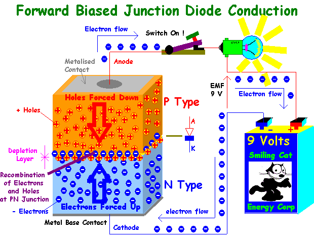
Conversely, if the battery polarity is
reversed, the positive holes will be attracted to the now negatively charged
Anode and the electrons will be attracted to the positive Cathode. Unlike the
previous forward biased condition, in which the depletion layer was
squashed together, now the width of the depletion layer increases. No
recombination can occur, and therefore a complete current path is not available.
Consequently, reverse bias results in blocked current flow.
In practice, conduction is relative.
Some current will flow in the reverse direction due to the small presence of
holes in N-Type material and electrons in P-Type material. In addition, surface
mechanisms for additional leakage may exist. In general, most P-N junctions
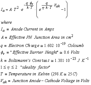
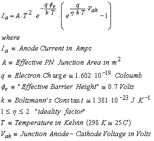
closely follow a I-V transfer function given by,
 …(1)
…(1)
Here
 refers to the current flowing from
Anode to Cathode,
refers to the current flowing from
Anode to Cathode,
 refers to the voltage from Anode to
Cathode.
refers to the voltage from Anode to
Cathode.
 is a “saturation current”
parameter relative to the particular diode (and is temperature dependant) and k
is a constant defined as,
is a “saturation current”
parameter relative to the particular diode (and is temperature dependant) and k
is a constant defined as,
 …(2)
…(2)
The constant
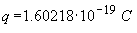 represents the electron charge,
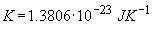 is Boltzman’s Constant and
 is an “ideality factor”
depending on the particular diode and semiconductor base.
is an “ideality factor”
depending on the particular diode and semiconductor base.
The PN-Junction diode can be used for RF
rectification up to about 100 MHz but becomes limited in its upper frequency
capability due to charge storage time. When electrons and holes “combine” in
the depletion time, it takes a finite time before they can “pass through”
and separate. This “charge storage” time causes the diode to remain
conducting for a short time even when it is reverse biased. Consequently,
rectification efficiency becomes impaired, falling to almost zero when the
charge storage time equals one half period of the RF signal frequency.
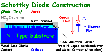
Schottky diodes are usually constructed
as from a Silicon N+ strongly doped material base with a thin N Type Silicon
Epitaxial layer on top. A non-ohmic metal contact is placed on top and this
creates a depletion zone at this junction. The difference in material “work
functions” creates a potential barrier, but in this case only majority
carriers are involved (electrons in both the N Expitaxial layer and the metal
contact). This results in an equivalent “P-N” junction but without the need
for electron-hole recombination. The previous recovery time delay is therefore
avoided, and the turn off time of a Schottky diode is limited only by its
internal capacitance and series resistance. Equivalent values of
 are typical for RF Schottky diodes,
compared to
are typical for RF Schottky diodes,
compared to
 for small signal junction switching
diodes like the leaded 1N4148 or its SMD BAV99 equivalent.
for small signal junction switching
diodes like the leaded 1N4148 or its SMD BAV99 equivalent.
|
|
The Schottky diode is used
as an RF Mixer and RF level detector well above 50 GHz. Different
metals define its “barrier height”, which is an indication of
the forward voltage needed to produce a defined current. Low
barrier devices draw 1 mA at ~200 mV. High barrier types might
require ~400 mV for 1 mA of current but have a higher reverse
breakdown limit, up to 70 V currently.
|
|
It is also possible to
make Schottky diodes from P-Type material. These tend to have low
reverse breakdown strength but can rectify with zero bias. They
are best suited for “square law” signal strength detectors,
which produce a voltage proportional to RF power.
|
|
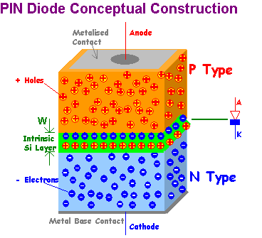
PIN diodes are almost the exact opposite
of Schottky diodes in that they seek specifically to have very long charge
storage times.
The P-Intrinsic-N or PIN
diode has a layer of pure (un-doped) intrinsic Silicon sandwiched
between the familiar P and N doped areas. This middle intrinsic
layer “traps” hole and electron charges and as a result, the
PIN diode takes a relatively long time to turn off, when reverse
biased. The amount of trapped charge depends on the current and
the volume of the intrinsic layer. Typical recombination times can
be in the order of microseconds. As a result, the PIN diode makes
a poor rectifier at RF, but can be made into a switch, or a
current controlled RF resistor.
|
|
Zener diodes and Avalanche diodes have
the same basic PN junction structure but operate with completely different
physical mechanisms.
All PN diodes are photosensitive to some
extent, but different semiconductor materials can modify sensitivity and
wavelength specificity.
Electrical characteristics can often be
classified into the following convenient categories,
- Static
DC Characteristics
- Dynamic
(Incremental, Audio) Characteristics
- AC
Characteristics (RF Small Signal Behaviour)
Static
 and
and
 relationships are a useful “first
step” in appreciated a given device’s electrical behaviour. Simple passive
components such as resistors have a simple linear relationship between
quantities of voltage and current, but most semiconductor devices don’t.
Instead they have an added dimension of non-linear electrical behaviour.
relationships are a useful “first
step” in appreciated a given device’s electrical behaviour. Simple passive
components such as resistors have a simple linear relationship between
quantities of voltage and current, but most semiconductor devices don’t.
Instead they have an added dimension of non-linear electrical behaviour.
In many cases, these simple DC
characteristics can be considered in terms of yes/no logic. For example a
reverse biased diode can be considered to be “non conducting”, and a forward
biased diode as “conducting”. Further we can add some if’s and buts for
further clarification. For example a reverse biased diode is “non
conducting” unless its voltage breakdown limit is exceeded. Then it is
conducting again. Equally, a forward biased diode “conducts” if its forward
bias exceeds a certain threshold. An in both cases, some temperature dependency
may exist.
 …(1)
…(1)
5.2.2
Advanced PN Junction Diode Thermal-Electrical Model
A more accurate theoretical expression
for the PN Junction diode’s thermal-electrical behaviour is,
 …(2)
…(2)
Equation (2) provides an accurate model
for forward biased diodes.
This can be used in the forward biased
region but fails miserably in predicting reverse bias behaviour in any real PN
junction diode. For example, the term
 tends to zero quite quickly as
 . Equation (5) could therefore be simplified,
5.2.3
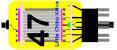
Example 1N4148 PN Junction Diode Data (Fairchild Semiconductor)
Fairly common small signal Silicon
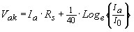
Junction diodes include the 1N914, 1N4148, BAV70 etc. These have a typical Vak{Ia}
exponential DC characteristic curve
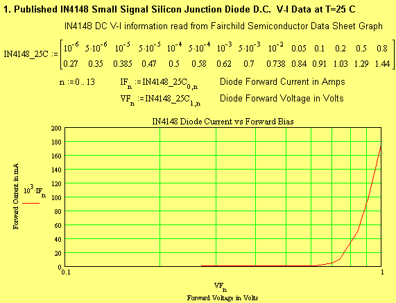
Silicon diodes are often referred to as
having a “turn on voltage” of about 0.7 V, but this “threshold” is
largely an illusion.
is relative to the current at which this
“turn on” knee is defined as can be seen in the following graph.
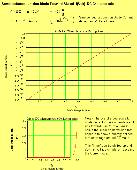
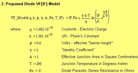
This MATHCAD demonstration uses the
following equations and constants,
The first graph displays the diode
current I in a log scale, and no evidence of a “turn on voltage knee” is
visible. However, the use of a linear scale in the second graph gives the
appearance of a clearly defined turn on region at about 0.7 Volts. Is this a
real characteristic or an illusion based on the choice of scale? Interestingly,
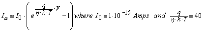
if we rewrite equation (1) as
 …(2)
…(2)
This form “suggests” the existence
of a “turn on voltage”
 but the value is slightly higher
than the value that might be interpreted from the preceding MATHCAD graph.
Although the form of equation (2) could be used, it is less compact than
equation (1) in that an additional coefficient
but the value is slightly higher
than the value that might be interpreted from the preceding MATHCAD graph.
Although the form of equation (2) could be used, it is less compact than
equation (1) in that an additional coefficient
 is introduced without any
corresponding new information or detail.
is introduced without any
corresponding new information or detail.
Sometimes it is convenient to separate
the diode DC equation into simper regions and make some reasonable
approximations, as previously. A
typical diode has
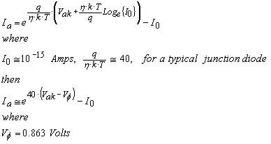
 at room temperature. Also, the exponential is usually very large or very small
compared to 1 for most bias voltages. If we consider three regions for Forward
Bias, Zero Bias and Reverse Bias defined as,
at room temperature. Also, the exponential is usually very large or very small
compared to 1 for most bias voltages. If we consider three regions for Forward
Bias, Zero Bias and Reverse Bias defined as,
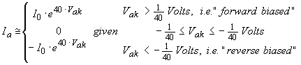 …(3)
…(3)
This three-region split is sufficiently
accurate for most purposes and is much easier to remember.
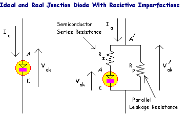
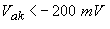
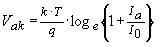
Real diodes have additional DC
imperfections that modify their electrical behaviour. Although the voltage
directly across the junction can be expected to comply accurately with equation
(1), some additional voltage drop will occur between the junction and the diode
lead due to the finite series resistance of the semiconductor material. This
voltage loss will equal
 where
where
 represents the total series
resistance. In addition, surface imperfections may cause additional leakage
currents to flow, which will be especially apparent in the reverse biased
condition. For example, an insulation resistance as high as 1,000 Meg-Ohms at
–10 V reverse bias will create a leakage current of 10 nA, i.e. much greater
than the expected diode saturation current of 10-15 Amps (0.001 pA!).
Equation (2) could therefore be re-expressed as,
represents the total series
resistance. In addition, surface imperfections may cause additional leakage
currents to flow, which will be especially apparent in the reverse biased
condition. For example, an insulation resistance as high as 1,000 Meg-Ohms at
–10 V reverse bias will create a leakage current of 10 nA, i.e. much greater
than the expected diode saturation current of 10-15 Amps (0.001 pA!).
Equation (2) could therefore be re-expressed as,
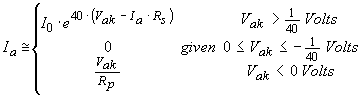 …(3)
…(3)
The expression for Anode current
 based on applied forward bias has
no closed form solution, and will require numerical methods to find an accurate
solution especially if the voltage drop caused by series resistance
based on applied forward bias has
no closed form solution, and will require numerical methods to find an accurate
solution especially if the voltage drop caused by series resistance
 is large.
The solution for device voltage
 based on forward current
 is straightforward in comparison,
 …(4)
…(4)
Semiconductors can withstand an
electrical field up to a point where electrons or holes are ripped from their
outer orbits. When this occurs, the freed charges allow conduction and large
currents could flow. If the current is limited, this “breakdown” mode could
be used to advantage as a way of providing voltage regulation. Diodes used for
voltage regulation are called “Zener diodes”, but most are actually
“Avalanche diodes”. This breakdown mechanism occurs at a clearly defined
threshold, but is slightly temperature dependent. The construction is similar to
a standard PN junction diode, except that doping arrangements are chosen that
define a required breakdown limit.
Avalanche behaviour usually dominates
for reverse voltages greater than 5 Volts. Junction diodes can easily achieve
breakdown voltages up to 1000 Volts and higher (1N4007 1 Amp 100 V rectifier as
an example). Diodes designed for voltage regulation are typically available in
steps from a few volts up to 50 Volts or more. An interesting phenomena
regarding noise generation also occurs in this region. Several mV of wide band
noise may be observed after avalanche behaviour occurs. In some cases, this may
be useful as a source of broad-band noise, or in other cases it may be an
unwelcome nuisance.
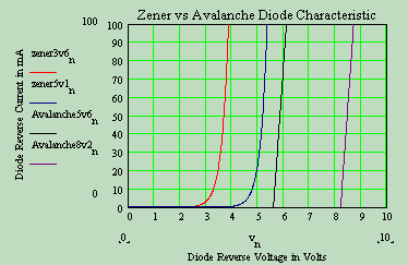
True Zener diode behaviour is based on
quantum mechanical effects, which become effective at lower breakdown voltages
in highly doped diodes. A comparison of typical V-I curves shows a clear
difference between the two modes of voltage regulation,
|
|
Zener
diodes usually have breakdown ratings below 5.6 Volts, whilst
Avalanche diodes typically exists with breakdown voltages above
5.6 Volts. The Zener behavior shows a rounded “knee” and
therefore provides relatively poor voltage regulation unless the
supplied diode reverse current is kept constant. The Avalanche
region in contrast is very sharp, and shows a slope that depends
mainly on the diodes’s series resistance
 .
.
|
|
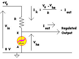
In most applications, IC based voltage
references are the preferred option for accurate voltage regulation and have
excellent temperature and stability. “Zener” diodes are still useful as a
low cost method for clamping unwanted signal voltage “spikes”. They are also
used as simple voltage references in less critical applications.
A
series resistor is used to limit current to an appropriate value,
but this current must be greater than any additional current
required from its regulated output. This “parallel” regulation
mode is not as energy efficient as other methods, and as such is
only used in low current situations involving several milli-amps.
|
|
5.4.1
More General Diode Equation For Thermal Prediction
A more accurate theoretical expression
for the PN Junction diode’s thermal-electrical behaviour is,
 …(5)
…(5)
This can be used in the forward biased
region but fails miserably in predicting reverse bias behaviour in any real PN
junction diode. For example, the term
 tends to zero quite quickly as
 . Equation (5) could therefore be simplified,
 …(6)
…(6)
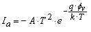
Let use define a reference room
temperature of
 and a resulting reverse anode
current
and a resulting reverse anode
current
 measured under this temperature
condition. The ratio of reverse current
measured under this temperature
condition. The ratio of reverse current
 at temperature
 to this reference reverse current
 at temperature
 would then be,
 …(7) Note – a very poor estimator of reverse diode current!
The reverse leakage current for a PN
Junction diode typically doubles for every 8-degree rise in temperature.
Equation (7) clearly does not display this relationship, and in fact suggests a decrease
in current for rising temperature. A more practical equation for reverse bias
leakage current is,
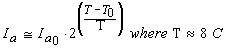 …(8)
…(8)
In addition, real PN junction diodes
display an increase in reverse leakage current with increasing reverse bias that
appears close to a straight line fit when the current is plotted on a
Logarithmic axis.
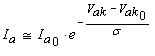 …(8)
…(8)
Note: The negative
sign is included on the exponential exponent as
 for reverse biased operation.
It would seem that a dual variable
equation could be formed from the product of equation (7) and (8), i.e.
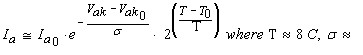 …(9)
…(9)
This new expression appears to have no
dependency on reverse bias voltage, which we know from measurement to be untrue.
Equation (6) will however demonstrate a general temperature dependency and will
therefore be pursued.
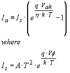
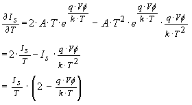
5.4.2
The Effect Of Temperature On The PN-Junction Diode’s Forward Voltage
The PN Junction diode has an explicit
temperature dependant term
 in its exponential V-I equation.
The effect of this would be to cause the current to change over temperature when
Vak is held constant, or for Vak to change when Ia
is held constant. However it is not the only temperature dependant term
in its exponential V-I equation.
The effect of this would be to cause the current to change over temperature when
Vak is held constant, or for Vak to change when Ia
is held constant. However it is not the only temperature dependant term
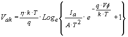
We will first re-write equation (1) so
that the diode forward bias voltage Vak is the subject
 …(5)
…(5)
Let us now differentiate equation (5)
where the temperature T is treated as the main variable,
 …(6)
…(6)
Consequently, we find that
 …(7)
…(7)
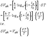
Equation (7) shows us that the
percentage change in absolute temperature equals the percentage change the
diode’s forward voltage drop, for a given fixed anode current.
At room temperature, T = 273K + 25C =
298K. A 1 degree change in temperature will therefore cause in a voltage change
of 2.35 mV for a diode biased with a current corresponding to an initial forward
voltage of 0.7 Volts.
Differentiating with respect to
temperature
Making Vak the subject
In many cases it is useful to know the
incremental current and or voltage behaviour of a given component so that its
small signal, low frequency characteristics can be ascertained. This analysis is
usually provided for the forward bias case.
 …(4) (for the purpose of this
analysis the relationship will be defined)
…(4) (for the purpose of this
analysis the relationship will be defined)
Differentiating with respect to voltage
we find,
 …(5)
…(5)
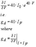
The “dynamic conductance”
 is directly proportional to the
junction diode’s forward bias current
is directly proportional to the
junction diode’s forward bias current
 and since resistance is defined as
the reciprocal of conductance we can also state,
and since resistance is defined as
the reciprocal of conductance we can also state,
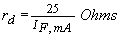 …(6)
…(6)
where
 . The junction diode can now be seen to provide a current dependent conductance
or resistance to small signal perturbations compared to its forward bias current
. The junction diode can now be seen to provide a current dependent conductance
or resistance to small signal perturbations compared to its forward bias current
 . We can also gain some insight into its non- linear properties in the forward
bias region by expanding equation (4) as a Taylor series,
. We can also gain some insight into its non- linear properties in the forward
bias region by expanding equation (4) as a Taylor series,
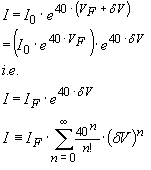 …(7)
…(7)
In this case
represents a small perturbation in
voltage around a given forward bias voltage
. Also note the n=1 tern corresponds to the previous expression for the dynamic
conductance
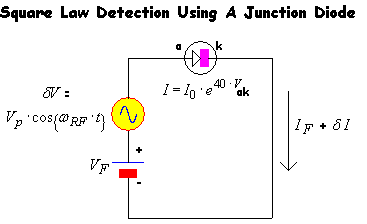
 . The n=2 term is also of interest for small signal detection and frequency
mixing. In this case
. The n=2 term is also of interest for small signal detection and frequency
mixing. In this case
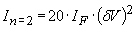 …(8)
…(8)

From equation (8)
where
 , therefore,
…(9)
The average current can be found by
integrating equation (9)
ignoring the cosine term and subtracting
the forward bias current,
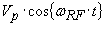
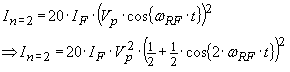
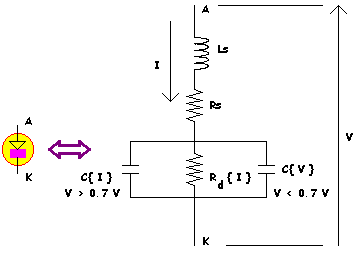
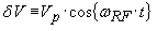
·
Ignore
Junction Capacitance
·
Ignore
Stored Charge
·
Ignore
Lead Inductance
·
Forward
Biased Junction Diodes Exhibit Current Dependent Capacitance
·
This is
Due To Charge Stored in The Junction
…(6)
Consider
the hypothetical Junction Diode
V ~ 0.7 V, I = 10 mA -> 0 mA, Time
 to remove this charge and turn off,
ó
C{ 10 mA } = 57 pF !!
(Note that the reverse capacitance
for such a diode might only be < 2 pF!! )
(Note Also – This Capacitance
Will Be In Parallel With Rd = 2.5 Ohms)
·
Can Be
Found From V{I} Curve Fit
·
Usually
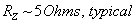
~ 5 Ohms or so for 1N4148 etc
·
Requires
High Reverse Voltage To Remove Charge Due To Rs
·
Diode Has Current Dependent
Dynamic Resistance Rd.
·
Diode Has Voltage and Current
Dependent Parallel Capacitance C
·
Diode Construction Also Has
Series Ohmic Resistance Rs
·
Package Has Lead Inductance Ls
|
|
Composite Junction
Diode Model
A reversed biased junction (and
Schottky) diode will exhibit classical “soft” varicap behaviour given by,
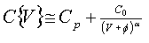 …(5)
…(5)
The coefficients can be determined by DC
curve fit approaches and an accurate match is usually obtained.
Note: Some Hyper Abrupt varicap diodes
may exhibit a negative Cp !!!
Semiconductors
had shown non linear properties such as rectification up to this point in time,
but the domain of signal amplification belonged to the vacuum tube triode,
tetrode and later the pentode. The vacuum devices had evolved significantly with
time, and became small enough to operate as hearing aid amplifiers and operate
from voltages as low as 9 Volts. They still required a heated (red) hot cathode
filament, which only served to
waste energy and shorten battery life.
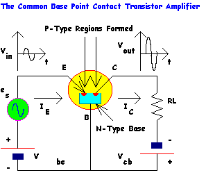
The
idea of a “solid state” amplifying device remained elusive until Schottky
and his team at Bell labs finally resolved previous failed attempts at
semiconductor based amplification. The structure they invented was based on a
single Germanium crystal mounted on a metal electrode with two closely spaced
gold metal strips pressed on to its surface. These formed the “Emitter” and
“Collector” terminals, and the metal mounting plate formed the “Base”.
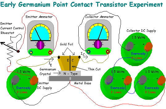
This
early experimental transistor had a common base current gain of about 2, and
although this was a very low value of amplification even by the standards of the
time, in was nonetheless evidence of amplification potential. Commercial
interest in manufacturable devices followed immediately, and many experimental
“point contact” germanium devices were produced. These used a similar
construction to their point contact diode predecessors, but were difficult to
manufacture as the two wire “whiskers” had to be placed within less than
th of a millimetre of each other for transistor action to occur.
Point
contact transistors were unusual in so far as they exhibited a common base
current gain greater than one, but could still be used in common emitter
configurations with appropriate bias. They had a Noise Figure in excess of 30
dB, which by today’s standards is abysmal, but could operate up to several MHz
due to the low self-capacitance of their contact leads. Although demonstrated in
a working computer application, they did not find their way into commercial
radio applications, and lasted only a few years before ousted by the Germanium
Bipolar Junction Transistor (BJT).
The Germanium Point
Contact Transistor could achieve a common base current gain
between 2~3 times, a voltage gain up to 500 times, and a power
gain in the order of 1000 times (30 dB), given ideal conditions.
However they were mechanically and thermally fragile, required
critical bias control and could only handle a few mA of current at
several volts. Their physics of controlling surface current flow,
it is said, remains unsolved to this day.
|
|


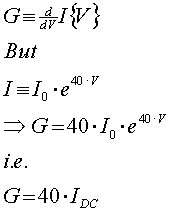 …(3), However
R = 1/G so….
…(3), However
R = 1/G so….
