Figure 7.1 Transformer Coupled Audio Amplifier.
For a verbal description click here.
Chapter 7 Transistorized Consumer Equipment.
7.1 Audio Amplifiers.
7.2 Radios and tuners.
7.3 Things you should leave alone.
Chapter 7.
Transistorized Consumer Equipment.
As you read in the foreword of this book it has been repurposed from a university textbook to a web publication whose target audience is more likely to be home experimenters and hobbyist. Therefore this chapter is about consumer grade electronics rather than exotic devices that may be found in a scientific research laboratory.Back to Fun with Transistors.
Back to Fun with Tubes.
Back to Table of Contents.
Back to top.
7.1 Audio Amplifiers.
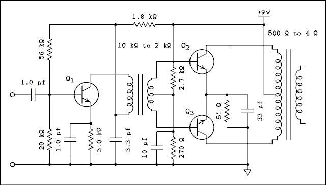
The term "audio amplifier" can cover a multitude of sins and in this section we shall cover the most important of them. There are thousands of variations on the basic audio amplifier so only a few representative samples can be given here.Transformer Coupled Audio Amplifier.
The very first audio amplifiers employing transistors were designed as the audio section in transistor radios. Figure 7.1 is an example.
Figure 7.1 Transformer Coupled Audio Amplifier.
For a verbal description click here.
Although this circuit is very old dating back to the dawn of the transistor age it still exists in vintage radios and phonographs and is occasionally used in new equipment.Transformer coupling was used because early transistors had low current gains. Transistors are current devices unlike tubes which are voltage devices. Note that both transformers are impedance step-down which translates to current step-up. Those transistors needed all the help they could get and the transformers provided it.
Note. The values given in the circuit are NOT from a vintage radio but have been designed to work with modern silicon transistors. If you were to construct this circuit using 2N3904s or any other small silicon NPN transistor it has a high probability of working and delivering approximately 250 mW, a little more on 12 volts.Although the transistors are transformer coupled the failure analysis given in section 6.1 for the common emitter configuration mostly applies here. The main difference is that in the push-pull pair consisting of Q2 and Q3 the collector voltage will mostly be at Vcc for all failure modes except an open transformer winding. That case will be identical to that for an open collector resistor. For the single ended amplifier of Q1 the 1.8 k ohm resistor will be the collector load for DC and the failure modes will be almost the same. The upper base biasing resistor is effectively returned to the collector for DC but the effect of this will be small for a failure mode analysis.In vintage equipment using germanium transistors there will be a thermistor in parallel with the resistor that is equivalent to the 270 ohm resistor. In most vintage circuits the capacitor across this resistor has been omitted. This omission likely slightly reduces power output and increases distortion. There was already so much distortion in these vintage circuits the designers probably felt that a little more wouldn't be noticed.
A variation of the transformer coupled amplifier was seen in line operated table radios from the mid 1970s onward. It came close to being the transistor equivalent of the all American five tube radio but never really caught on.

Figure 7.2 Line Operated Transformer Coupled Amplifier.
For a verbal description click here.
This circuit was made possible by the fact that high voltage power transistors had come down in price sufficiently to make the circuit practical. The output transformer would likely be a 5 k ohm to 4 ohm unit not unlike the ones used in tube radios. The transistor would be mounted on a heat sink of some kind maybe the metal chassis of the radio. Q5 served a double purpose being simultaneously the audio power output stage and voltage regulator for the radio circuitry.The diode half wave rectifies the line voltage and the rectifier's output is filtered by the 30 uf capacitor. The ripple on the output is calculated by starting with the equation,
i = C dV/dt (Eq 7.1) First we mentally change the derivative to delta V / delta t and change the case of the current symbol, then solve the equation for dV.DV = Dt I/C (Eq 7.2) Where DV is the change in voltage over a finite time, Dt is the time interval, I is the DC load current, and C is the capacitance of the capacitor in farads.DV = 16 e-3 seconds x 20 mA/30 uf = 10.7 volts. 16 e-3 (16 milliseconds) is approximately the length of one cycle in north America.The calculated peak of the 120 volt line voltage is 170 rounded to 3 digits. The calculated peak to peak ripple of 10.7 volts means that an average DC voltage of 165 volts is reasonable. This voltage value was used to design the transistor circuit. Because a transistor is a constant current device, similar to a pentode tube, voltage changes of 10 volts peak to peak will not produce any significant changes in collector current. The output transformer responds to changes in current so the hum level will be almost undetectable.
The voltage divider consisting of the 15 k ohm 2 watt and the 1.3 k ohm resistors form a voltage divider which places the base of Q5 at approximately 12.6 volts. The emitter will then be at 12 volts. The * 620 ohm resistor is the closest standard value that will produce 20 mA of emitter current in Q5. The resistor must be recalculated to account for the current drawn by the converter and IF stages of the radio. Let's say that the current drawn is 5 mA. Then the resistor has to conduct 15 mA to common to set the emitter current to 20 mA. The resistor value is given by 12 v / 15 mA = 800 ohms. The closest standard value is 820 ohms which means that the emitter and therefore the collector current of Q5 will be a shade low. In a real circuit the emitter voltage may be set a little higher and an additional RC filter stage inserted to ensure there will not be any positive feedback which could result in motorboating of the radio.
The above mention motorboating could be a fault of the circuit if the capacitor from the emitter of Q5 to ground were to develop a high effective series resistance (ESR).
If the emitter capacitor were to short Q5 would draw too much current, overheat, and short. This would apply the full line voltage peak to the converter and IF circuits thus cooking the entire radio and likely making its repair uneconomical. Only a restorer of antiques would be interested in it after such a catastrophic failure.
Transformerless Amplifier.
Below is the circuit that was used for power amplifiers from the earliest days of transistors to some time in the early 70s.
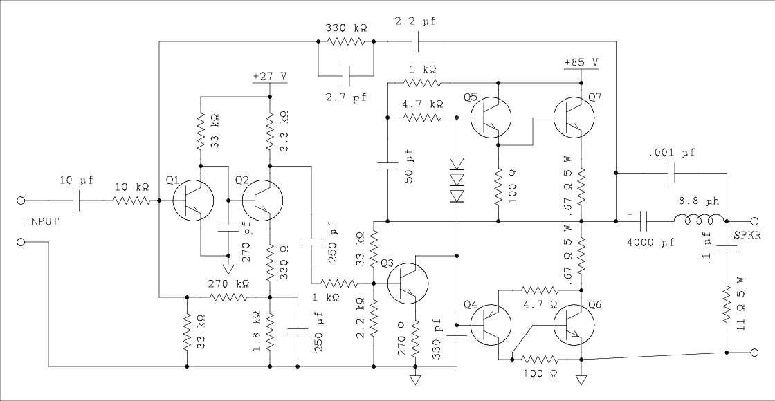
Figure 7.3 Transformerless Amplifier from the 1960s.
For a verbal description click here.
This circuit actually has 3 feedback loops. 1) An AC negative feedback loop around the entire amplifier from the positive side of the 4000 uf capacitor, which is often called the amplifier midpoint, through the 2.2 uf capacitor and the parallel combination of the 330 k ohm resistor and the 2.7 pf capacitor to the base of the first transistor. 2) A DC coupled negative feedback loop from the amplifier midpoint through a 33 k ohm resistor to the base of the transistor that would be Q3 if I had remembered to number them. 3) An AC coupled positive feedback loop from the amplifier midpoint through the 50 uf capacitor to the junction of the 1 k ohm and 4.7 k ohm resistors.The first two transistors on the left are in a stabilized configuration identical to that of Figure 6.18. As pointed out in chapter 6 the failure of the second transistor's collector resistor can cause the phase of the amplifier to reverse while it does continue to amplify to some degree. This would change the negative feedback to positive and the amplifier would oscillate at some frequency, most likely high, possibly ultrasonic.
If ultrasonic the oscillation is likely to do serious damage to speakers before being detected. The output transistors would most likely blow.
The second feedback loop stabilizes the amplifier midpoint at 1/2 of the Vcc supply. If the 33 k ohm or the 270 k ohm resistor opens the midpoint will go up to very near Vcc. If the 2.2 k ohm resistor opens the midpoint will come down to be very close to zero. If the 250 uf capacitor between Q2 and Q3 shorts Q3 will be driven to high collector current and the amplifier midpoint will be reduced in voltage. I think the 1 k ohm resistor in series with the 250 uf capacitor is meant to reduce the effect of such a short to prevent damage to the rest of the amplifier.
Note there are three diodes in series with the collector of Q3. Note also that the base of the top darlington pair is connected above the diodes while the base of the lower complementary darlington pair is connected below the diodes. These diodes are to temperature compensate the idling current of the outputs. They are usually very near the heatsink or may even be thermally bonded to it. If one or more of these diodes shorts the effect might not be noticed for some time. Its main effect would be to reduce the idling current of the outputs likely to zero. The resultant distortion would be compensated for and covered up by the large amount of negative feedback. The user may perceive that the amplifier doesn't sound right but may not be able to put his finger on the problem.
If one of these diodes opens, all four transistors in the output stage as well as the two 0.67 ohm resistors are in for a cooking. If you replace the two resistors and four transistors without finding out what made them cook the replacements will cook just as the originals had.
If any one of the four transistors shorts it will most likely take the other three with it. This leaves the same symptom as an open diode but one of the four transistors shorting was the precipitating event. You are likely to find all four transistors open. That is because the initial short caused excessive current to flow which shorted another transistor and then the enormous amount of current melted the transistors open before the main fuse had time to blow. I have even seen the small leads on the driver transistors between the transistor header and the PC board burned in two. Repairing such an amplifier can be a game of Russian roulette. You replace all four transistors and the two resistors and check everything else you can think of, close your eyes and apply the power. The problem with this circuit and others like it is you can't fire it up with the expensive high power transistors removed. You have to put it all back together and hope.
The third feedback loop is more commonly known as bootstrapping. The 50 uf capacitor couples AC signal from the midpoint to the junction of the two resistors. The effect is to tremendously increase the effective value of the 4.7 k ohm resistor. As the mid point is driven up and down by AC signal the left end of the 4.7 k is also driven up and down. The voltage drop across the resistor is very nearly constant. Constant voltage means constant current. Instead of behaving like a resistor it behaves like a constant current source for the collector of Q3. This has the effect of increasing the gain of Q3 and reducing distortion in the three diodes. A short in the 50 uf capacitor would place the top transistors in cutoff which would allow the midpoint to be pulled down near zero. If the capacitor were to open the bootstrapping effect would be lost. This would increase the amount of distortion but the global feedback would tend to cover it up. Depending on how demanding a listener the owner is the amplifier might be brought in for service only to have the repair man say "It sounds alright to me." On the other hand the owner may not notice that anything is wrong and the problem could go undetected for years.
Short circuit protection.
Adding the protection circuitry makes this the schematic of the much celebrated Heath AR-15.

Figure 7.4 Schematic Diagram of the Heath AR-15.
For a verbal description click here.
The added parts that make up the protection circuit may be hard to find. It consists of the series combination of two zener diodes connected anode to anode and a 100 uf capacitor. The literature I have for the amplifier does not reveal the voltage of the zener diodes. If a short is placed across the output the high current will cause a large AC voltage to be developed across each of the two 0.67 ohm resistors. This voltage also appears across the series combination of the two zener diodes and the capacitor.Suppose there is a short and the input signal is telling the output to swing positively. The emitter of the top output will swing positive creating a larger than normal voltage drop across the top 0.67 ohm resistor. The positive going swing on the emitter of the top output transistor was caused by a positive going swing on the collector of Q3. Remember that there is a short on the amplifier output and the 4000 uf capacitor prevents any significant swing on the amplifier mid point. When the voltage across the 0.67 ohm resistor is large enough the left hand diode will go into zener breakdown and the right one into forward breakdown. This will prevent the voltage at the collector of Q3 from going any higher thus limiting the current to a safe value. When the output tries to swing negatively the lower 0.67 ohm resistor conducts a high current and the voltage at the collector of Q3 is negative going. The right hand diode goes into zener breakdown while the left hand one goes into forward breakdown. This prevents the collector of Q3 from going any more negative thus limiting the current.
The truth was, and is, that this protection circuit didn't work very well. That's why I had the "pleasure" of observing the leads of the driver transistors having been melted, or perhaps vaporized, after a catastrophic failure.
Heath, About 8 years later.
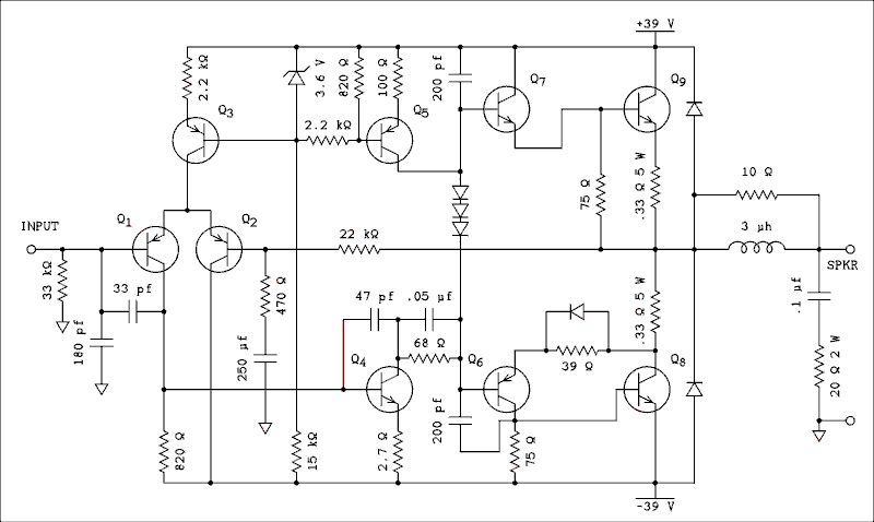
Figure 7.5 Improved Transformerless Amplifier from the 1970s.
For a verbal description click here.
Here is a circuit from the third decade of transistorized consumer equipment. Its main improvement is DC coupling throughout including the global feedback loop. Also a transistor (active) current source has replaced the bootstrapped resistor. The global negative feedback is applied to one base of a differential pair with input applied to the other. There is a current source in the emitters of the differential pair. It operates from symmetrical power supplies so the midpoint is held at zero. Almost any circuit fault will cause a large DC offset which can destroy a speaker system in pretty short order if there is no protective fuse.The chief difficulty with this kind of circuit is that any fault anywhere will propagate around the feedback loop and every voltage will be out of whack. There are often clues. Say the midpoint is locked to the positive rail. You should find that the base of Q2 is more positive than the base of Q1. Because these are PNP transistors Q2 will be in cutoff and Q1 will be taking all of the current of the current source Q3. This will pull the collector of Q1 higher than normal and pull the base of Q4 higher, increasing its collector current. This will be trying to pull the three diodes down but it can't because the amplifier is at positive rail. The feedback is telling the amplifier to go negative but something is keeping it from it. It could be a short in any one of the three transistors Q5, Q7, Q9, or the 200 pf capacitor. Q4 could also be open causing this symptom.
This circuit suffers from many of the same problems as Figure 7.3 with the additional ones introduced by DC coupled feedback.
Both of these circuits have current limiting circuitry to protect the amplifier against a short in the speaker wiring. These circuits work in the same way as current limiting in a bench power supply. The voltage drop across the low ohm resistors in the output is sensed and if it exceeds a certain value the current supply to the bases of the power transistors is shut down.
Because the circuit of Figure 7.4 is dc coupled the current limiting circuitry must be DC coupled and somewhat more elaborate.
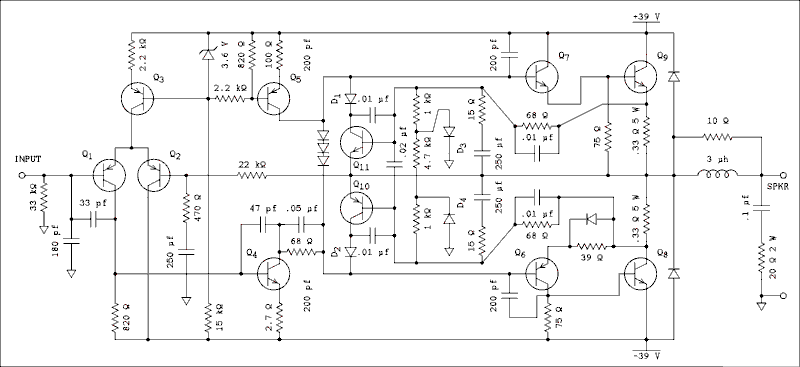
Figure 7.6 Heath AA2015 and other similar models.
For a verbal description click here.
The limiting transistors are Q10 and Q11. Their emitters are connected to the amplifier midpoint. Diodes D1 and D2 disconnect the current limiting circuitry when no limiting is taking place. The connections from the top and bottom ends of the sense resistors may appear to be rather complicated but if you mentally strip it all away, basically the top of the top 0.33 ohm resistor connects to the base of Q11 and the bottom of the bottom 0.33 ohm resistor connects to the base of Q10. The network of resistors, capacitors, and diodes appears to serve the main purpose of preventing oscillation when current limiting is in effect.On the positive half cycle if the load is drawing too much current Q11 is turned on and its collector current takes current away from the base of Q7 reducing the output to a safe level. On the negative half cycle Q10 takes current away from Q6 limiting the current.
Stop the presses, it isn't quite that simple. Those two diodes D3 and D4 appear to add a lot of complexity but the limiter wouldn't work right without them. When there is no current limiting taking place everything is going up and down positive and negative with respect to ground. The drop across the 0.33 ohm resistors is small so the two 68 ohm resistors, the two .01 uf capacitors, the two 15 ohm resistors, the two 250 uf capacitors, (they are connected to the midpoint), the top end of the top 1 k ohm resistor, the bottom end of the bottom 1 k ohm resistor, Q10, Q11, and the three capacitors that are around Q10 and Q11, are all swinging up and down with the output signal.
But on the positive swing D3 is forward biased and holds the junction of the upper 1 k and the 4.7 k to near ground. This reverse biases the base emitter junction of Q11 which was already turned off but forward biases the base emitter junction of Q10 which turns it on. This might turn off Q6 and Q8 but they are already turned off. On the negative half cycle of normal output Q11 is turned on. This has no effect until current limiting kicks in.
If there is a short or too many speakers connected to the amplifier, Q11 will be turned on as explained above. If Q10 were not already on the voltage at the collector of Q5 would be pulled down which would turn on Q6 and Q8. Q4 and Q5 are both current sources so their voltage can be easily pulled around. This would bring about the destruction of Q6, Q7, Q8, and Q9, instead of protecting them. Q10 and Q11 being turned on at the same time prevents this from happening. The similar event occurs on the negative swing.
Current limiting circuitry is not likely to fail because it rarely if ever turns on. If prolonged current limiting should overheat either or both Q10 or Q11 causing it(them) to short the amplifier might appear to work at very low volume settings but distort at even moderate listening levels. Such a fault might be hard to find if you fail to check the current limiting components.
Integrated Circuit Amplifiers.
I recently had on my bench a home theater amplifier made by Sony. It had discrete complementary output transistors but the rest of the circuitry was inside a medium power integrated circuit. Fault detection circuits found a DC offset and would not connect the speakers while indicating an error on the front panel display. The offset was not large being about 1/4 of the Vcc and Vee supplies. The power transistors had normal values of Vbe indicating neither an open or short. My only alternative was to replace the IC. That turned out to fix it. Because of minimum order requirements I had to buy 3 of the ICs. Such is the plight of someone who does not operate a professional service shop.Then there are those amplifiers that are one great big IC for each channel. Before ordering these expensive parts perform the "what is it being told to do" test. These are really nothing but high power op amps and they will be treated as such in this explanation. If the output is locked to the positive rail and the inverting input is more positive than the noninverting input the output is being told to go negative. If the output is locked to the negative rail and the inverting input is negative with respect to the noninverting input the output is being told to go positive. In either of these cases the op amp is not doing what it is being told to do so it must be defective.
On the other hand if the output is locked to the positive rail and the inverting input is negative with respect to the noninverting input the amplifier is being told to go positive. If the output is locked to the negative rail and the inverting input is more positive than the noninverting input the amplifier is being told to go negative. In either of these cases the amplifier is doing exactly what it is being told to do. The fault lies with the surrounding circuitry that is doing the telling. There are so many variations on these circuits that it is impossible to give any examples.
Back to Fun with Transistors.
Back to Fun with Tubes.
Back to Table of Contents.
Back to top.
7.2 Radios and tuners.
The All Japanese Six.
The 6 transistor radio which I shall call the All Japanese 6 (AJ6) uses 3 of its transistors in the audio section, another as the converter and the remaining two in the IF amplifier.Note. The first transistors were mass produced by Texas Instruments and their engineers designed the first practical transistor radio. It was made under contract by a company in Illinois for a time. However as has happened so many times over the years since 1952 the Japanese were able to make it at less cost which drove American manufacturers out of the transistor radio business. Even though it isn't "all" Japanese I choose to call it the AJ6 in the same way as the 5 tube radio that really was all American was called the All American 5 (AA5). I do this with apologies to the states of Texas and Illinois.
One of my professors told the following joke. "Whenever an American company comes out with a new product, within one week the Russians have invented it first, and within two weeks the Japanese are making it cheaper." I have no knowledge of the USSR claiming to have invented the transistor radio first but there is no doubt that the Japanese did make it cheaper. Now it's the Chinese but that's another story for another time.
The diagrams below were obtained from this website. The diagrams have been redrawn to avoid any copyright problems.
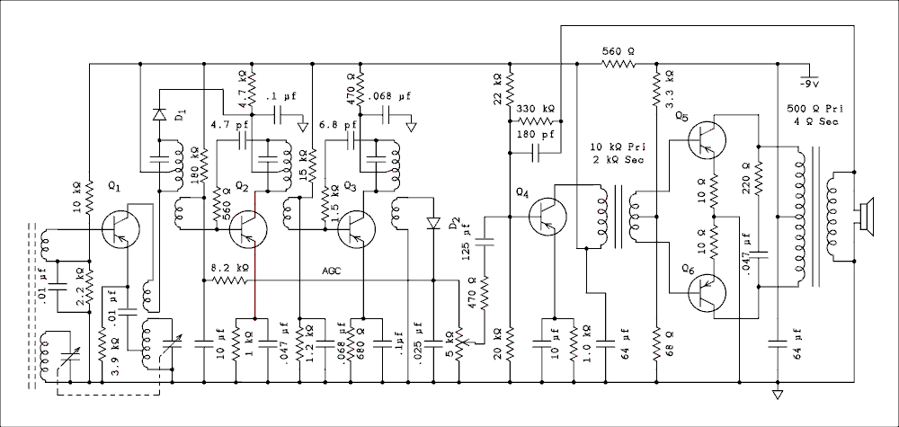
Figure 7.7 Voxson Model 762.
For a verbal description click here.
These diagrams give no clue as to the year of introduction. They all use germanium PNP transistors so the late 1950s or early 60s seems to be a good guess.The Converter.
The station signal is picked up by the ferrite rod antenna and signal is coupled into the converter, Q1, by a coil that consists of a few turns wound between the turns of, or over, the grounded end of the main tuned winding. The transistor uses series fed constant voltage biasing. The 10 k ohm and 2.2 k ohm resistors provide the bias voltage to the transistor. The emitter resistor sets the collector current. The .01 uf capacitor keeps the low end of the base winding at RF ground.In the collector of Q1 the tickler coil for the oscillator and the primary of the IF transformer are connected in series. Signal from the tickler coil is magnetically coupled to the resonant coil and a tap on this coil couples signal of the proper phase through the .01 uf capacitor to the emitter of Q1. The resonant coils of the ferrite antenna and the oscillator coil are tuned by the two sections of the tuning capacitor.
The IF (Intermediate Frequency) Amplifier.
The difference signal between the oscillator and station signal, 455 kHz, is coupled to the primary of the input IF transformer. Vcc is fed to the mid-tap on the IF transformer primary and the collector is connected to the end of the winding nearest the tap. This prevents the low impedance at the collector of Q1 from lowering the Q of the tuned circuit.The function of D1 is unclear. Its anode is connected to the high impedance end of the primary of the input IF transformer while its cathode is connected to the mid-tap on the interstage IF transformer. The Q point program tells us that the no signal collector current of Q2 is 212 microamps which gives a drop across the 4.7 k ohm resistor of approximately 1 volt. If a very strong nearby station were to be tuned in the peak RF voltage at the anode of D1 could exceed 1.1 volts but it is hard to say exactly what would happen. A strong signal would reduce the forward bias on Q2 bringing the voltage on the cathode of D1 closer to its DC anode voltage. The DC voltage at the mid-tap of the interstage transformer might be reduced which would reduce the gain of Q2 but the top end of the input transformer is a high impedance point which has many more turns between it and the mid-tap than there are between the collector end and the mid-tap. The cathode of the diode would have to drive the 4.7 k ohm resistor. It seems more likely that the signal on the primary of the input transformer would just be clipped distorting the modulated signal from the station.
The base winding of the input IF transformer couples signal to the base of Q2. Q2 is biased from the -9 volt line through a 180 k ohm resistor and AGC (automatic gain control) is applied through an 8.2 k ohm resistor. The AGC voltage is derived from the cathode of the detector D2 so it is positive going. This will reduce the collector current of Q2 reducing its gain. This is the only point in the radio where closed loop AGC is applied. (Note. As speculated above the signal rectified by D1 may be forward gain control but its function seems doubtful.) The primary function of the 4.7 k ohm resistor and 0.1 uf capacitor is to decouple the collector of Q2 from the minus nine volt line. The collector of Q3 is decoupled by the 470 ohm resistor and 0.068 uf capacitor.
The interstage IF transformer couples signal from the collector of Q2 to the base of Q3. The output IF transformer couples signal from the collector of Q3 to the detector, D2. The base of Q3 is biased by the voltage divider consisting of the 15 k ohm and 1.2 k ohm resistors. The 680 ohm resistor in the emitter sets the collector current. The 0.068 uf capacitor bypasses the cold end of the base winding on the interstage IF transformer and the 0.1 uf capacitor bypasses the emitter of Q3.
Both Q2 and Q3 are neutralized by the series combination of a resistor and small capacitor connected between the top of the IF transformer primary and the base. The use of a resistor is quite rare. Usually only a capacitor is seen. Early transistors had a substantial reverse voltage transfer ratio, hre. This consisted of the capacitance between collector and base but also an electric field effect which altered the forward voltage drop across the base emitter junction as the collector voltage changed. The resistors apparently were used to neutralize the real part of hre while the capacitors neutralized the imaginary part. This was evidently an example of thorough engineering which other companies found to be unnecessary. That would seem to point toward this being an early design. More about this when discussing figure 7.8.
Detector and AGC.
D2 half-wave rectifies the voltage on the secondary of the output IF transformer. The 0.025 uf capacitor smoothes out the 455 kHz ripple component while leaving the audio uneffected. The DC component which is proportional to the strength of the received station's signal is fed through an 8.2 k ohm resistor to the cold end of the base winding on the input IF transformer. A 10 uf capacitor filters out all audio from the AGC signal so just the strength of the station's signal will affect the gain of Q2. As the signal from the station gets stronger the DC voltage applied to the right end of the 8.2 k ohm resistor grows more positive. An increasing positive voltage reduces the bias on Q2 which reduces its collector current thus lowering its gain. Both the DC and audio are applied to the top of the 5 k ohm volume control. The signal from the wiper also contains a reduced version of the DC and audio. The 125 uf capacitor blocks the DC from the base of Q4.The Audio Amplifier.
The base of Q4 is biased by the voltage divider consisting of the 22 k ohm and 20 k ohm resistors. The collector current of Q4 is set by the 1.2 k ohm resistor and this resistor is bypassed by the 10 uf capacitor. Signal from the collector of Q4 is coupled by the interstage audio transformer to the bases of Q5 and Q6. The low end of the primary of the interstage transformer is bypassed to ground by a 64 uf capacitor. This capacitor in conjunction with the 560 ohm resistor serves to decouple Q1 through Q4 from the effects of the audio power output transistors Q5 and Q6.Q5 and Q6 have base bias applied through the secondary of the interstage transformer from the resistive voltage divider consisting of the 3.3 k ohm and 68 ohm resistors. Q5 and Q6 each have their own 10 ohm emitter resistors. This will provide some automatic collector current balancing effect not available if a single emitter resistor had been used for both transistors. Leaving these two resistors unbypassed also provides some negative feedback to the output stage. Signal from the collectors of Q5 and q6 is coupled by the output transformer to the speaker. The 220 ohm resistor and 0.047 uf capacitor roll off the high frequencies and stabilize the global negative feedback loop. This feedback is taken from the secondary of the output transformer back to the base of Q4 through the parallel combination of a 330 k ohm resistor and a 180 pf capacitor.
Comments.
The thoroughness of the neutralizing of the IF stages and the use of negative feedback in the audio section indicates that considerable thought was put into the design of this radio. It's hard to believe all that was used to drive a 2 inch speaker. Perhaps the design was lifted from an AC operated table radio with a larger speaker.Another Example.

Figure 7.8 Sanyo Super-Six.
For a verbal description click here.
The converter.
This circuit is similar to the Voxson radio above but there are also notable differences. Feedback from the tuned winding of the oscillator coil is fed through a 0.003 uf capacitor to the cold end of the base winding on the ferrite rod antenna. This strikes me as a questionable design change because it is certain to result in a stronger signal from the local oscillator being radiated from the radio as compared to designs where the feedback is coupled to the emitter of the converter transistor. 4 of the 17 6 transistor radio circuits I found have oscillator feedback taken to the base of the converter transistor. The rest take the feedback to the emitter.IF Amplifier.
Q2 and Q3 are neutralized by capacitors only which is far more typical of transistor radio designs. Also there is no decoupling for Q2 and Q3.AGC.
The major difference is in the AGC system. The top of the output IF transformer secondary connects to the cathode of a diode D1 and the bottom connects to one end of a 0.01 uf capacitor. Instead of being connected to ground the bottom end of the winding is connected to the same voltage divider which biases the base of Q2. This divider consists of a 90 k ohm and an 18 k ohm resistor. This sets the base bias for Q2 as well as the reference for the detector at approximately -1.5 volts. This bias point is bypassed for both audio and Rf by a 10 uf capacitor.The signal from the anode of the detector, D1, is partially filtered by the 0.01 uf capacitor which has its other end connected to the bottom of the IF secondary coil. Additional filtering is provided by the 200 ohm resistor and another 0.01 uf capacitor. At this point there is DC for AGC plus detected audio. The DC is filtered by a 5.6 k ohm resistor and the 10 uf capacitor in the emitter of Q2.
The AGC detector like any electrical source has two outputs. The positive side is the bottom end of the IF transformer secondary which is labeled AGC. The negative output is the bottom end of the 5.6 k ohm resistor. This source of DC is floating, not tied to ground anywhere, and is connected between the emitter and base of Q2. As the signal from the station becomes stronger the positive voltage applied between emitter and base becomes larger which takes away from the normal negative bias for a PNP transistor. The collector current of Q2 is reduced which reduces its gain. But in addition the voltage at the emitter becomes less negative.
Note that the bias for the base of Q3 instead of being derived from a voltage divider as in the circuit above, comes from the emitter of Q2. As the emitter voltage of Q2 becomes less negative so does the base voltage of Q3. This reduces its collector current which reduces its gain. AGC action in this radio would be much improved as compared to the one above because AGC is applied to both IF stages Q2 and Q3 instead of just to Q2.
Audio is coupled from the junction of the 200 ohm and 5.6 k ohm resistors through a 10 uf capacitor and a 1 k ohm resistor to the top of the volume control. This is labeled VR on the schematic and does not have an entry in the parts list. The wiper of the control feeds through another 10 uf capacitor to the base of Q4. Note that the designer of this radio took measures to keep DC levels off of the volume control. This reduces crackling when the control is rotated.
The Audio Amplifier.
The audio section has a few differences from the circuit above but is mostly similar. There is a 0.005 uf capacitor across the primary of the driver transformer. If the transformer is actually a 10k primary to 2k secondary the roll-off frequency is 3180 Hz which seems low even for a pocket radio. The 9 volt battery line is decoupled from the supply for Q1 through Q4 by a 200 ohm resistor and a 50 uf capacitor. The emitters of Q5 and Q6 are tied together and connected to ground through a single 10 ohm resistor. There is no negative feedback around the audio amplifier in this radio.There is not a thermistor in either circuit selected as representative of 6 transistor radios. This may indicate that these are both early designs. Owners of radios of this type found they would stop playing if left on a beach blanket in the hot sun for several hours. The radios were found to be working upon arrival home. The problem was instability of the operating point of some of the transistors. The two most vulnerable stages were the converter, Q1, and the push-pull outputs, Q5 and Q6.
At elevated temperatures the transistor's current gain would increase causing it to go into saturation and stop oscillating. The cure for this was to make the parallel combination of the two biasing resistors in the base very approximately equal to the emitter resistor. This appears to have been done in both designs shown above. The result of an overheated push-pull pair was distorted sound and a quickly run down battery. As the transistors heated up their current gain would increase causing them to draw more current which heated them up more causing more current etc. etc. In line powered radios this runaway condition usually resulted in cooked transistors. In a battery powered radio a run down battery was usually the only result. Several repeats of this incident resulted in unhappy customers and eventually the engineers added the thermistor to compensate for wide temperature changes.
What can go wrong?
After the manufacturers made their radios able to work at the beach there really wasn't much left to go wrong. Low voltages and currents didn't put much stress on resistors, capacitors, and transistors. When a radio turned up at a service shop it was usually because of being dropped into the family swimming pool or overboard from the family boat. In such cases it was not economical to repair because the cost would exceed the price of a new radio. Indeed by the late 60s a six transistor radio could be had for 5 or 6 dollars.At this writing the very first transistor radios made in USA are 60 years old. If they haven't already these will soon become quite valuable as rare antiques because there were so few made.
Meanwhile the transistor radios of today use the same ferrite antenna, tuning capacitor, and IF transformers, but the transistors have been incorporated into a 16 pin DIP. If a true 6 transistor radio lands on your bench it is most likely that the owner, sometimes you, wants it restored to operation for sentimental reasons. What voltage, current, and power, couldn't do to these radios, time has. The electrolytic capacitors will most certainly need to be replaced. In early transistors the mechanical connection between the leads and the germanium crystal wasn't very good and often failed. In most cases the radio will still play but the sound contains a most annoying crackling that is usually not effected by mechanical shock. Germanium transistors are available from specialty suppliers. A Google search should turn them up. I once went so far as to reengineer a transistor radio for silicon NPN transistors. It's not a job I would recommend to anyone.
The volume control in these radios is usually not the enclosed potentiometer we are accustomed to seeing in other equipment. The carbon element is glued to the circuit board and the wiping contact runs around it as the knob is turned. At the counter clockwise end of its rotation part of the wiper moves a contact opening the connection to the 9 volt battery. This leaves the carbon ring vulnerable to being damaged or at least getting dirty. Either one will result in a crackling sound when the control is rotated. If this occurs some control cleaner applied to the carbon ring will fix the problem. If the control has been damaged it will have to be replaced. The best source is probably another radio. I have no experience to offer on how to remove these rings.
Another source of crackling is the tuning capacitor. These capacitors are inside a plastic box and as far as I know opening the box is an irreversible process. To save space these capacitors have very thin layers of plastic between the plates. It is not unusual for the plastic to have worn through in a few places allowing the plates to make electrical contact. Replacing the capacitor is the only fix for this. Fortunately in most radios the tuning capacitor is easily removed and if you can obtain a matching capacitor, easily replaced.
As mentioned above the modern pocket radio contains a DIP IC instead of transistors. However, the tuning capacitor appears to have changed little if at all over the last 50 years. If all else fails, one of these IC radios could be a source of parts to repair an AJ-6.
Car Radios.
AM transistorized car radios are only slightly different from home AM radios. Three major differences are; They are with few exceptions tuned by variable inductors rather than variable capacitors, the intermediate frequency is 262.5 kHz, and the audio output is capable of delivering a watt or more. Much more in some cases. The FM stereo section is pretty standard.The hardest part of repairing car radios is getting them out of the car and then back in after repair is complete. Modern low voltage high current power supplies are sufficient to power one while it is on the test bench. In some cases the speaker or speakers are mounted in another part of the car, such as in the door panels but any small set of speakers can be substituted for troubleshooting purposes.
One complaint may be that there is excessive ignition noise and alternator hum in the radio. This problem is very difficult to troubleshoot because it can't be tested outside of the car. In older radios power is fed into the radio through feed-through capacitors which in car radio parlance are known as spark plates. These are usually found in tube radios in an era when low impedance feed-through capacitors had not yet been developed. A spark plate is a square of metal which is connected to the hot power lead and insulated from the radio chassis with a sheet of mica. There is little to go wrong with such a device except corrosion at the point where the power lead connects to the plate. In modern transistorized radios feed-through capacitors will be found instead of the older technology.
AM/FM Stereo Car Radios.
This book is primarily aimed at those repairing or restoring vintage equipment so little time will be spent on this subject. Other than the differences noted above for AM radios there is virtually no difference between a car radio and a home AM/FM stereo receiver. With the exception of the 120 VAC power supply of course. High power car stereos require more supply voltage than the 12 volts of the car's electrical system. If only the available 12 volt supply were used the highest peak-to-peak voltage across the speaker would be approximately 22 volts using a bridge amplifier. Based on a 4 ohm speaker the power calculates out to about 15 watts. While this would be plenty for any sane person those car stereos that you can hear booming from 2 blocks away are running several hundred watts. To obtain that much power they have to use Vcc supplies of 50 or 100 volts. These comparatively high voltages are obtained from an inverter circuit which is basically a silicon version of the vibrators used in tube radios of old.AM/FM Radios.
An AM/FM radio may be a portable, small table, clock radio, or car radio. Separate transistors are used for the AM and FM frontends. The low cost of transistors and high cost of switches is what makes this economically possible. Band switching is accomplished by switching on the Vcc to the frontend which is desired and switching off the Vcc to the other one. This can be done with a simple single pole double throw switch. Each mixer is coupled into the IF strip through the appropriate IF transformer. AM uses an intermediate frequency of 455 kHz while FM uses an intermediate frequency of 10.7 MHz.In the IF strip the FM and AM IF transformers have their primaries and secondaries wired in series to the base or collector of each IF transistor. The highest frequency transformer, 10.7 MHz FM IF, is closest to the transistor. The AM IF usually needs only 2 stages and the signal is taken off for detection after passing through this many transistor stages. The FM signal usually needs a total of 4 stages so the IF strip continues with only 10.7 MHz transformers after the AM takeoff point. Some radios may only have a total of 3 IF stages. The last stage of the IF strip is overdriven to remove amplitude variations which contain no intelligence.
The FM signal is demodulated by a circuit known as a ratio detector. The circuit is shown below.
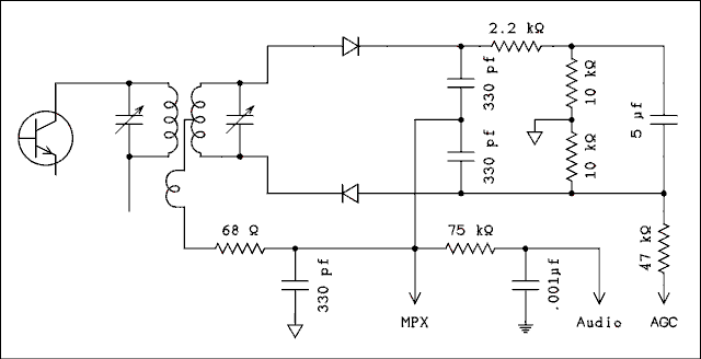
Figure 7.9 Ratio Detector.
For a verbal description click here.
There are three coils inside a discriminator transformer. (Note; even though the circuit is a ratio detector the transformer goes by the name of the other detector circuit which is a discriminator. The discriminator circuit is almost never used because of its poor AM rejection. But the transformer which is identical for both circuits still carries the name.) Now, where was I? Oh yes, 3 coils. The primary coil which is in the collector of the last IF transistor is tuned to the center of the FM IF, 10.7 MHz. The secondary which is center-tapped is also tuned to the center frequency. The third coil known as a tertiary winding is magnetically coupled to the primary but is untuned.Imagine for a moment that the tertiary winding has no voltage across it. The voltages at the top and bottom of the secondary are 180 degrees out of phase with each other. There will be a positive voltage at the cathode of the top diode and a negative voltage at the anode of the bottom diode. The polarity of the DC voltages are determined by the direction of the diodes not by the phase of the RF signals. These voltages will be filtered by the 330 pf capacitors. These voltages will cause current to flow through the two 10 k ohm resistors. (Let's simplify the explanation by pretending that the 2.2 k ohm resistor doesn't exist. The imbalance it introduces can be compensated for by slightly off-tuning the secondary of the transformer.) As the junction of the two 10 k ohms is grounded the voltage at the center-tap will be zero. Without the tertiary winding it would stay like that regardless of the input frequency.
The current which is induced in the tertiary winding is in phase with the current which is induced in the secondary winding. That is because both currents are being induced from the primary winding.
The tertiary winding is untuned and it has a self resonant frequency which is much higher than 10.7 MHz. Thus it appears inductive and the voltage is leading the current induced in it by 90 degrees. The bottom of this winding is very nearly at ground potential so the voltage applied to the center-tap of the secondary leads the current by 90 degrees.
Because the secondary is tuned to resonance at 10.7 MHz the voltage from the center-tap to the top is in phase with the current and the voltage from the center-tap to the bottom is 180 degrees out of phase with the current. Let us say for the sake of argument that the RF voltages across the top half of the secondary, the bottom half of the secondary, and the tertiary winding are all equal in amplitude and equal 10 volts. This condition is shown in the phasor diagram in Figure 7.10(a).

Figure 7.10 Phasor Diagrams of Discriminator Transformer Voltages.
For a verbal description click here.
The voltages across the tertiary winding and the top half of the secondary add as to the voltages across the tertiary and the bottom half of the secondary. This addition is shown in Figure 7.10(a). The voltage at the top of the secondary is 14.14 volts at an angle of 45 degrees while the voltage at the bottom of the secondary is 14.14 volts at an angle of 135 degrees. Note that both voltages still have equal amplitude although the relative phase angle has been altered. The diodes recover only amplitude information not phase information. Therefore the DC voltages at the cathode and anode of the top and bottom diodes respectively will be equal in value and opposite in sign. (+14.14 volts at the top and -14.14 volts at the bottom). Note that the DC and audio output from the detector is taken from the center-tap of the secondary. The tertiary winding has a minute amount of reactance at audio frequencies.Now suppose that the frequency shifts upward. The phase of the voltage at the top end of the secondary will shift negatively because the resonant secondary now appears capacitive. Voltage lags current in a capacitive circuit so the phase will shift and let's say it shifted by -45 degrees as shown in figure 7.10(b). The voltage at the top of the secondary is now 7.653 volts at an angle of 22.5 degrees. The voltage at the bottom of the secondary is 18.478 volts at an angle of 112.5 degrees.
Remember that the two 10 k ohm resistors are holding the voltages across them equal and balanced to ground. Phasors represent the peak value so the voltage between the anode of the lower diode and the center-tap is 18.478 volts with the center-tap positive with respect to the diode anode. The voltage between the upper diode cathode and the center-tap is 7.653 volts with the cathode positive with respect to the center-tap. The total voltage is 26.131 volts. Each 10 k ohm resistor will have 13.0655 volts across it. The voltage at the center-tap will be 13.0655 v - 7.653 v = 5.4125 volts. Note that for an increase in frequency the output of the detector goes positive which is desirable for tuning meters and automatic frequency control (AFC).
When the frequency goes below center by the same amount it went above center the numbers are the same but all signs are reversed.
I wonder if anyone noticed the discrepancy with the numbers. When the incoming frequency is at the exact center the total voltage across the two 10 k ohm resistors was 28.28 volts and at a frequency that will give a 45 degree phase shift the voltage was 26.131 volts. If the voltage of the tertiary winding is decreased to 1 volt the total DC is 20.1 volts at center frequency and 20.05 volts at a frequency that gives a 45 degree phase shift. Decreasing the phase shift to 30 degrees gives 20.1 v and 20.08 v respectively. Reducing the phase shift and tertiary voltage reduces the amount of recovered audio. Clearly the designers of ratio detectors have to make some compromises to obtain a practical audio level and acceptable distortion.
There are no large currents or voltages in this circuit which reduces the probability of component failure. Resistors and capacitors can simply fail from old age. The most likely one to fail from this cause is the 5 μf capacitor which is a low voltage electrolytic. This capacitor in conjunction with the 2.2 k ohm resistor set the AM rejection. If the electrolytic should dry out and its value be reduced the AM rejection of the receiver will be considerably poorer than when the set was new. Do not assume that if 5 μf is good that 10 μf is better. The impedance and time constant of the circuit consisting of the 2.2 k ohm resistor and 5 μf capacitor in conjunction with the Q of the transformer secondary set the best value of AM rejection. Changing the value of the capacitor will reduce the AM rejection of the detector. In this particular case the substitution of a 4.7 μf capacitor would probably be acceptable especially since 5 μf capacitors are no longer made.
Note: In diagrams of the Ratio Detector you are likely to find in other textbooks the 2.2 k ohm resistor will be split between the top and bottom of the circuit. The designers of this circuit are taking the AGC voltage from the bottom end of the 5 μf cap. My best guess is that if there were a resistor between the diode and this cap there would be an additional RC time constant in the AGC loop which might render it unstable.The two 10 k ohm resistors are 5% in table radios and are often 1% in High fi tuners. If one of them were to increase in value, a common result of old age, this would cause you to alter the tuning of the secondary of the discriminator transformer in an attempt to balance the circuit at center tuning. The effect of this would be to decrease the dynamic range of the detector possibly introducing a considerable amount of distortion.If you think the detector is misaligned refer to the alignment procedure in the FM Tuner section below. References to the stereo light and tuning meter won't apply to a portable or table radio but the sound will be the same.
FM Tuners.
There is so much variation in circuitry among various tuners that it is impossible to give any detailed schematic diagrams. An FM tuner has the following sections. RF amplifier, Mixer and local oscillator, linear IF amplifier, limiting IF amplifier, FM detector, and stereo multiplex demodulator.The RF amplifier operates in the frequency range between 88 and 108 MHz. The physical layout is even more critical than the component values. The simple act of bending a transistor to a more upright position could seriously degrade the performance of the tuner. If there is nothing wrong in the RF and mixer/oscillator section, don't touch it. If a transistor is burned out in this section and must be replaced your odds of ever getting it working again are small.
The linear section of the IF amplifier permits information for a signal level meter and AGC to be derived, usually from a simple diode detector.
The limiting section of the IF amplifier derives a signal which has a constant output level regardless of changes in the input signal. This is not done by AGC but by simple hard clipping. This is usually done within one or more integrated circuits. If the tuner is more than 20 years old these circuits may be very hard or impossible to find. Most all modern tuners use factory tuned LC filters or fixed tuned ceramic or crystal filters. In general such devices are not bothered by component replacement. Should one of these filters be found to be defective, and the tuner is old the chances of it playing again are small.
Detector Alignment.
CAUTION! Even high quality FM tuners in the transistor age use the same tiny transformers as their little brothers. The slugs in these have an obvious slot and they are very hard to turn. You may be tempted to use a metal screwdriver. DON'T DO IT! The slot will break out and the slug may break into several pieces rendering the chances of a successful repair even lower. These slugs are held in place with paraffin. A little gentle warming with a hair dryer will permit them to be turned safely with an alignment tool.Unless the tuner on your bench has been in the hands of someone who tightened up all the loose screws the IF and detector really won't need much if any alignment. In every old tuner I have seen the detector was slightly misaligned. You shouldn't need to turn the alignment slug more than 1/2 turn and more likely it will require less than a quarter turn.
The evidence for a misaligned detector is found by tuning across a strong local station which has only very weak signals nearby. When the detector is properly aligned you will observe three distinct listening peaks, not peaks on any meter. As you approach the signal you will begin to hear audio and it may not be distorted but it may be mixed with a little noise. The tuning meter will read quite low. As the tuning meter rises the sound will grow quite distorted. As you continue tuning the distortion will clear and the tuning meter will be at its peak. The stereo light will most likely come on. As you continue to tune the sound will once again grow distorted, the tuning meter will drop, and the stereo light will go out. The distortion will clear but the audio will be a bit noisy, and the tuning meter will read quite low.
A misaligned detector will give you two peaks and it may be ambiguous as to which one is the right one. Make small changes in the discriminator transformer or quadruture coil and tune across the station until you observe the signature of a properly aligned detector described above. If a symmetrical triple peak can't be obtained it may indicate trouble in the detector, or an IF that is seriously out of alignment.
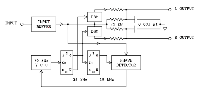
Figure 7.11 Block diagram of MC1310.
For a verbal description click here.
The input buffer provides a high input impedance to the chip while providing a low output impedance to drive all the internal circuitry. The entire composite stereo signal is applied to all internal circuit blocks and each one uses what it needs and ignores the rest. This eliminates the need for tuned circuits and LC filters.The internal 38 kHz carrier is generated from the 19 kHz pilot by a phase locked loop. The 76 kHz VCO (voltage controlled oscillator) is divided by two by a JK flip-flop and then by two again by another flip-flop. This yields 19 kHz which is fed to the phase detector. The phase detector picks out the 19 kHz pilot tone and locks the VCO to it.
When the two input signals of a phase detector are at 90 degrees and the same frequency the DC output voltage is zero. When the two signals are in phase the output is positive and when the two are 180 degrees out of phase the output is negative.
The VCO is designed and adjusted so when the DC input voltage is zero its frequency is 76 kHz. When the voltage is negative the frequency is lower than 76 kHz and when the input voltage is positive the frequency is higher.
If the frequencies differ by say 1 Hz the output of the phase detector is 1 Hz. This will cause the VCO to be frequency modulated at 1 Hz and when it falls on 76 kHz the VCO will lock onto the pilot tone. The tuning range of the VCO is small so it won't lock onto musical notes in the program material.
The phase difference of the two 19 kHz signals is 90 degrees but at twice the frequency, namely 38 kHz the phase difference becomes 180 degrees. The 38 kHz signal between the two flip-flops is 180 degrees out of phase with the carrier that is required to recover the difference signal. A reversal in phase will flip the phase of the recovered difference signal. That is, The difference signal will become -L + R. When the 38 kHz signal is fed to a DBM (doubly balanced mixer) it will use the 23 to 53 kHz double sideband signal to recover the -L + R signal which when combined with the composite signal through the two 75 k ohm resistors will derive the left channel. The not Q signal from the flip-flop is 180 degrees out of phase with the Q signal so when it is applied to another DBM it derives the L - R signal. When this signal is combined with the composite signal it derives the right channel signal.
What is a doubly balanced mixer?
Note: In the discussion below the terms sum frequency and difference frequency are used. Do not confuse these terms with the terms difference signal and sum signal. The sum signal is the L + R signal and the difference signal is the L - R signal. A sum frequency is a new frequency resulting from two frequencies being added together. A difference frequency is a new frequency resulting from two frequencies being subtracted one from the other. I promise to always say exactly what I mean and mean exactly what I say.A DBM produces the sum and difference frequencies the same as any other mixer. If two signals of 6 kHz and 4.5 kHz are injected into a DBM the output is 1.5 kHz and 10.5 kHz. But the two original signals of 4.5 kHz and 6 kHz are canceled out by the circuitry and do not appear in the output. The truth is that the internal circuitry of the two DBMs is no different from the circuitry of the phase detector. They are the same circuit serving different functions. This makes chip manufacturing easier because it becomes a series of modules that are connected together before final packaging.The 23 to 53 kHz double sideband signal combines with the 38 kHz signal to produce audio from 50 Hz to 15kHz which is the recovered difference signal. Also the original L + R sum signal combines with the 38 kHz signal to produce sum and difference frequencies which is a whole new set of frequencies in the range of 23 to 53 kHz. If the original difference signal were not canceled out by the DBM these frequencies would combine, beat together, to produce all sorts of weird effects.
The 76 kHz VCO is an RC controlled Multivibrator with the resistor and capacitor outside the IC. Part of the resistor is usually a trimmer resistor to set the frequency of the oscillator. The four 75 k ohm resistors are internal but the 0.001 uf capacitors must be supplied on the outside.
The output of the IC is not line level so gain stages must be provided before going to line output jacks. Many tuners have elaborate filters to make sure no frequencies above the audio band escape from the tuner. If the 19 or 38 kHz signals were to appear at the output with any appreciable amplitude they would beat with the bias oscillator in a tape recorder and produce beat frequencies, tones, in the audio band. These tones would not be heard when listening to the radio but would be heard in the recording.
What can go wrong?
If there is no output from the chip it is most likely bad and must be replaced. A possible symptom is that there is audio but it is monophonic, the same signal from both channels. This can be tested for without having to rely on your ears. Connect the two channels to the X and Y inputs of an oscilloscope and be sure the station you have tuned in is transmitting stereo program material. If the output is monaural the scope will show a straight line at 45 degrees to the horizontal. If the signal is stereo the scope will show all kinds of random circles and ellipses.If the receiver is producing monaural try adjusting the trimmer pot in the frequency determining parts of the VCO. Many times this will fix the problem.
If one channel is dead check the gain stages that come after the demodulator chip.
If there is trouble in the filters and the user owns a tape recorder there may be beats in the recording that aren't heard in normal listening. Back to Fun with Transistors.
Back to Fun with Tubes.
Back to Table of Contents.
Back to top.
7.3 Things You Should Leave Alone.
You should leave the following items alone.
- VCRs.
- CD Players.
- DVD Players.
- Flat screen TVs.
You may break the "leave it alone" rule if all four of these conditions are satisfied.
- The item is not working at all.
- It is out of warranty.
- The service shop you took it to declined to work on it.
- You own the item.
When you have nothing to lose there is no risk and you might just get it working. But don't make any bets or hold your breath.
So what to do if you decide to open it up and have a look. Before removing the screws or prying up the tabs check the back, or the manual, if you still have it, for a reset button.
Assuming you manage to get it open without doing too much damage trace the AC power line. You might find a fuse and most likely it will be a solder in type and won't be the kind you can walk into a Radio Shack and buy. If the fuse is blown don't replace it just yet. Fuses do occasionally blow all by themselves but it is rare.
Keep following the AC trail. Depending on the size of the device you may or may not find a power transformer. But eventually you will find one or more diodes and a filter capacitor. Check them for shorts.
After the rectifier and filter you may find either an analog voltage regulator or a switch mode power supply. At this point the problem usually becomes getting at the components to figure out what is there let alone test and replace them. If the designers were thoughtful enough to realize that this part of the unit is field repairable the circuit boards may come out easily.
If you get this far without finding any fault temporarily solder in a fuse clip and insert a standard fuse of the proper current rating. If it blows you haven't found the problem. If it doesn't start checking around on the net to find the proper replacement. If you can find a way to safely anchor the fuse clip so it is not hanging from the leads on the PC board you may decide to leave it in place.
CD and DVD players will have two power supply lines a positive and a negative with respect to ground. VCRs and TV sets will have a multitude of voltages available from the power supply. TV sets are most likely to have no line frequency transformer but a switch mode power supply after a bridge rectifier and filter capacitor.
DVD and CD players and VCRs can have mechanical problems which can be difficult to diagnose without special test sets supplied by the manufacturer. VCRs often have small spring loaded switches that are meant to detect trouble in the mechanism and shut off the power or reverse the action to prevent damage. These switches are often not of the best quality and they end up being the cause rather than the cure.
Often the wisest decision is to walk away particularly if the thing doesn't belong to you. In the words of the song, "You've got to know when to hold em and know when to fold em."
Back to Fun with Transistors.
Back to Fun with Tubes.
Back to Table of Contents.
Back to top.