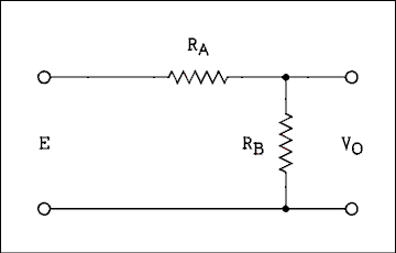
Figure 0.1, Voltage Divider Circuit.
For a verbal description click here.
Chapter 0 Electrical Fundamentals.
0.1 DC Circuits.
0.2 AC Circuits.
0.3 Power Supplies.
0.4 Bipolar Transistor Fundamentals.
0.5 Bipolar Transistor Circuits.
0.6 Operational Amplifiers.
0.7 Field Effect Transistors.
0.8 FET Circuits.
0.9 Vacuum Tube Fundamentals.
0.10 Vacuum Tube Circuits.
Chapter 0
Review of Fundamentals.
In order to understand the material in this book, the reader must understand certain fundamentals of electricity and electronics. The teaching of these fundamentals is far beyond the scope of this book. This chapter is merely a review. If the reader is not familiar with any of what is presented in this chapter, it is strongly urged that he or she supplement his or her knowledge by studying Electronics for Non-Engineers.Back to Fun with Transistors.
Back to Fun with Tubes.
Back to Table of Contents.
Back to top.
0.1 DC CIRCUITS.
Kirchhoff's voltage law states that the algebraic sum of all voltage drops around a closed loop is equal to zero.Kirchhoff's current law states that the algebraic sum of all currents flowing into a node is equal to zero.
The consequences of these laws for series circuits are a) the sum of all voltage rises is equal to the sum of all voltage drops, and b) the current anywhere in a series circuit is equal to the current anywhere else in the same circuit.
The consequences of Kirchhoff's laws for parallel circuits are a) the sum of all upward flowing currents is equal to the sum of all downward flowing currents, and b) the voltage across any element in the circuit is equal to the voltage across any other element in the same circuit.
Ohm's law states the relationship between voltage, current and resistance in an electric circuit.
V = I x R (Eq. 0.1) where V is voltage in volts, I is current in amperes and R is resistance in ohms.I = V/R (Eq. 0.2)
R = V/I (Eq. 0.3)
To properly apply Ohm's law it is necessary to use the resistance of a particular resistor, the current through that same resistor and the voltage across that same resistor.
When resistors are connected in series the total resistance is
RT = R1 + R2 + R3 + ... + Rn for any number of resistors in series.When resistors are connected in parallel the equivalent resistance is
1/Req = 1/R1 + 1/R2 + 1/R3 + ... + 1/Rn for any number of resistors in parallel.
Figure 0.1, Voltage Divider Circuit.
For a verbal description click here.
Figure 0.1 is of a voltage divider. RA and RB may be the equivalent of other resistors in series and/or parallel. The output voltage Vo is given byVo = E RB/(RA + RB) (Eq. 0.4) Thevenin's theorem states that a network with output terminals and is of any level of complexity, using resistors, can be reduced to one ideal voltage source in series with a single resistance.The ideal (Thevenin) voltage source is equal to the no- load output voltage of the original network.
The Thevenin resistance is equal to the resistance looking in at the terminals of the original network with all voltage sources replaced by shorts and all current sources replaced by opens.
Example 0.1.
Determine the Thevenin equivalent circuit of the network of figure 0.2.
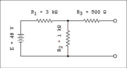
Figure 0.2, Circuit for Example 0.1.
For a verbal description click here.
Solution:
With no load connected to the output, there will be no voltage drop across R3. Therefore, the voltage across R2 will be the same as the output voltage. R1 and R2 make up a voltage divider. By equation 0.4 we haveVo = 48 v x 1 k ohm / (3 k ohm + 1 k ohm ) = 12 volts.
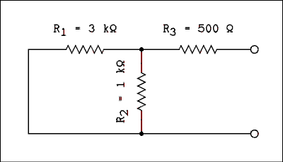
Figure 0.3, Network of Figure 0.2 with the voltage source replaced by a short.
For a verbal description click here.
If we replace the battery in figure 0.2 with a short and redraw the circuit we have the circuit of figure 0.3. The resistance looking in at the terminals is R1 in parallel with R2 and this combination in series with R3. R1 in parallel with R2 is R12 = 1/( 1/(1 k ohm ) + 1/(3 k ohm )) = 750 ohm. Now adding R3 in series we have 750 ohm + 500 ohm = 1250 ohm. The Thevenin equivalent circuit is shown in figure 0.4.
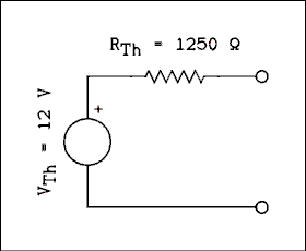
Figure 0.4, Thevenin's Equivalent Circuit of Figure 0.2.
For a verbal description click here.
There are many other methods of solving electric networks. A few of these are Norton's theorem, superposition theorem, loop equations, node equations and Y-delta transformation. If you do not understand these techniques, it will be necessary to take an introductory level course in electrical engineering.RC Time Constant.
If a capacitor C is being charged or discharged through a resistor R the time constant is given byT = R x C (Eq. 0.5) where T is time in seconds, R is resistance in ohms and C is capacitance in farads.T is the time required for a charging capacitor to charge up to 63.2 percent of its final voltage or for a discharging capacitor to discharge to 36.8 percent of its starting voltage.
Theoretically a capacitor will never get fully charged or discharged. As a matter of practicality a capacitor is considered to be fully charged or discharged after 5 x T seconds have elapsed.
Back to Fun with Transistors.
Back to Fun with Tubes.
Back to Table of Contents.
Back to top.
0.2 AC CIRCUITS.
All of the laws and theorems which apply to DC also apply to AC. In theorems stated in words replace the word "resistance" by the word "impedance". In equations, replace the symbol R by the symbol Z where Z = R + jX or Z = Z /_ ThetaA capacitor is an open circuit for DC but has reactance for AC. The reactance of a capacitor is
XC = 1 / (2 x Pi x f x C) (Eq. 0.6) where XC is the reactance of the capacitor in ohms, f is the frequency in hertz and C is the capacitance in farads.An inductor has a very low resistance for DC (ideally zero) but has reactance for AC. The reactance is given by
XL = 2 x Pi x f x L (Eq. 0.7) where XL is the reactance of the inductor in ohms, f is the frequency in hertz and L is the inductance in henrys.Back to Fun with Transistors.
Back to Fun with Tubes.
Back to Table of Contents.
Back to top.
0.3 POWER SUPPLIES.
Power supplies serve the purpose of changing the 120 volt AC line voltage to one or more useful DC voltage(s).
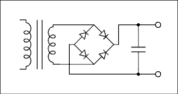
Figure 0.5, Full-Wave Bridge Rectifier Power Supply.
For a verbal description click here.
The circuit of a full-wave bridge rectifier is shown in figure 0.5. The no-load output voltage of this circuit is given byEM = EAC x Square Root (2) (Eq. 0.8) where EM is the no-load DC output voltage of the circuit and EAC is the RMS AC voltage across the entire transformer secondary.

Figure 0.6, Full-Wave Center-Tapped Rectifier Power Supply.
For a verbal description click here.
The circuit of a full-wave center-tapped rectifier is shown in figure 0.6. The no-load voltage of this circuit is given byEM = EAC x Square Root (2)/2 (Eq. 0.9) where EM is the no-load DC output voltage of the circuit and EAC is the RMS AC voltage across the entire transformer secondary.The ripple output from a full-wave rectifier power Supply operating on 60 Hz is given by
VR = EM / (200 x RL x C (Eq 0.10) where VR is the peak to peak ripple voltage of the power supply, EM is the no-load DC output voltage as given by equation 0.8 or 0.9, RL is the equivalent load resistance on the power supply in ohms and C is the capacitance of the filter capacitor in farads.Back to Fun with Transistors.
Back to Fun with Tubes.
Back to Table of Contents.
Back to top.
0.4 BIPOLAR TRANSISTOR FUNDAMENTALS.
All of the following discussion assumes the transistors are NPN. For PNP transistors, just reverse all voltages and currents.A transistor has three terminals. They are called emitter, base and collector. Internally the transistor is made up of three alternating layers of semiconductor material, for example, NPN. The emitter is one of the N layers, the base is the P layer and the collector is the other N layer. This means that there are two P-N junctions, one between the emitter and base and the other between the collector and base.
The normal way of biasing a transistor is to forward bias the base-emitter junction and reverse bias the collector-base junction. For an NPN transistor this means to connect a current source between emitter and base so as to run current into the base, and connect a Thevenin circuit between emitter and collector such that the collector is positive and the Thevenin voltage source is greater than 0.6 volts. Figure 0.7 shows the biasing circuit.
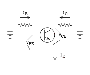
Figure 0.7, Ideal Biasing Circuit for an NPN Bipolar Junction Transistor.
For a verbal description click here.
The voltage between emitter and base VBE is about 0.65 volts. Some authors round this up to 0.7 while others round it down to 0.6 volts. Depending on the magnitude of the collector current the voltage between collector and emitter VCE will be anywhere between 0.1 volts and VTH.If VCE = 0.1 volts, the transistor is said to be in saturation. If VCE = VTH the transistor is said to be in cutoff. If 0.1 volts < VCE < VTH is true, the transistor is said to be in linear operation.
When the transistor is in linear operation the collector current is controlled by the base current. If the base current is zero, the collector current is zero because the collector base junction is reversed biased. As base current increases, the collector current increases. The current gain of the transistor is defined as follows.
Beta = IC / IB (Eq. 0.11) Therefore,IC = Beta x IB (Eq. 0.12) The emitter current is the sum of base and collector currents.IE = IB + IC (Eq. 0.13) Back to Fun with Transistors.
Back to Fun with Tubes.
Back to Table of Contents.
Back to top.
0.5 BIPOLAR TRANSISTOR CIRCUITS.
Figure 0.8 gives a practical biasing circuit for an NPN transistor. It will be easier to analyze this circuit if we reduce the voltage divider in the base circuit to its Thevenin equivalent circuit. This has been done in figure 0.9.

Figure 0.8, Transistor with Constant Voltage Biasing.
For a verbal description click here.
VBB = VCC x R2 / (R1 + R2)
And
RB = (R1 x R2) / (R1 + R2).
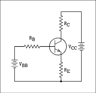
Figure 0.9, Constant Voltage Biasing Circuit with a
Thevenin's equivalent circuit replacing the
voltage divider in the base circuit.
For a verbal description click here.
If we write a loop equation around the base loop and substitute equations 0.12 and 0.13 we get this equation for the collector current.Exact form IC = Beta (VBB - VBE) / (RB + RE (Beta + 1)) (Eq. 0.14) If Beta is large or guessed at, and it is usually both, the collector current becomesFirst approximation IC = (VBB - VBE) / ((RB/Beta) + RE) Eq. 0.15 If RB / Beta << RE, as it sometimes is, the collector current becomes,Second approximation IC = (VBB - VBE) / RE (Eq. 0.16) There are three ways of injecting and recovering signals in a transistor amplifier. These are common emitter, common collector (emitter follower) and common base.Common Emitter Amplifier.
A common emitter amplifier is shown in figure 0.10. The common sides of the input and output are connected to the circuit ground. The emitter of the transistor is also connected to signal ground through a capacitor. The emitter is common to both input and output. The resistor on the right labeled RFS is the input resistance of the Following Stage. The voltage gain of this circuit isAV = - Beta x RL / hie (Eq. 0.17) where AV is the voltage gain, Beta is as defined above, RL is the parallel combination of all resistances connected to the collector of the transistor and hie is the input resistance of the transistor. hie is never given in transistor manuals. It can be found in manufacturers' data sheets but it varies quite a lot from one unit to the next, even of the same type number. As a very rough approximation hie = (1 volt) / IC, this approximation is not good enough to get an equation number.
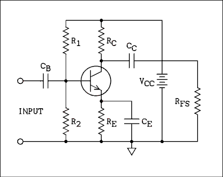
Figure 0.10, Common Emitter Amplifier Circuit.
For a verbal description click here.
The input impedance is equal to hie in parallel with the parallel combination of R1 and R2, The output impedance is equal to RC.If the emitter bypass capacitor is removed the gain becomes
AV = - RL / RE (Eq. 0.18) where RL is as defined above and RE is the emitter resistor.The input resistance is Rin in parallel with RB. Rin is given by
Rin = hie + Beta x RE (Eq. 0.19) The term Beta x RE is usually much greater than hie so the equation becomesRin = Beta x RE (Eq. 0.20) The output impedance remains equal to RC.The upper frequency limit of an amplifier is considered to be the frequency at which the output is 3 db down from the output at medium frequencies. This is variously known as the upper frequency limit, the upper 3 db frequency, the upper corner frequency, the upper cutoff frequency or the bandwidth. We will symbolize this frequency by fC.
fC = 1 / (2 x Pi x Rl x C) (Eq. 0.21) where RL is the parallel combination of RC and all other resistances connected to the collector in ohms and C is the total capacitance from collector to ground in farads.The Miller effect causes the input capacitance of an inverting amplifier to be much larger than the stray wiring capacitance. The Miller capacitance is given by
CM = CBC x (1 - AV) (Eq. 0.22) where CM is the Miller capacitance and CBC is the capacitance between collector and base of the transistor including wiring capacitance. Remember that in an inverting amplifier AV is a negative number.Common Collector (Emitter-Follower) Amplifiers.
The circuit of a common collector amplifier is shown in figure 0.11. Equations 0.14 through 0.16 may be used to calculate the collector current of this circuit.
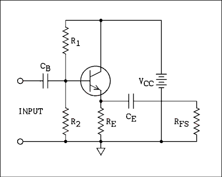
Figure 0.11, Common Collector (Emitter-Follower) Amplifier.
For a verbal description click here.
The voltage gain of this circuit is approximately equal to unity.The input impedance of this circuit is the parallel combination of Rin in parallel with both R1 and R2.
Rin = Beta x RL (Eq. 0.23) where RL is the parallel combination of all resistors connected to the emitter of the transistor.The output impedance of this circuit is RE in parallel with ROUT.
ROUT = RS / Beta (Eq. 0.24) where RS is the parallel combination of R1, R2 and Rg, the generator output resistance.Because the voltage gain is very close to + 1, equation 0.22 tells us that the Miller capacitance CM is essentially zero. Do not get the mistaken impression that the input capacitance is zero. There is always stray wiring capacitance.
Common Base Amplifier.
The circuit of a common base amplifier is shown in figure 0.12. The voltage gain is given by equation 0.17. The input resistance is approximately equal to hie / Beta. The output impedance is equal to RC.
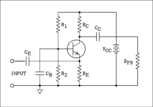
Figure 0.12, Common Base Amplifier.
For a verbal description click here.
The base of a transistor is physically between the emitter and collector. When the base is grounded (for AC), the base becomes an electrostatic shield between the emitter (input) and collector (output). Through careful circuit layout CEC the capacitance between emitter and collector can be made very small (of the order of 0.1 pf).A common base amplifier is noninverting. Equation 0.22 would actually give a negative input capacitance. This negative Miller capacitance will cancel with positive (real) stray circuit capacitance and it is possible to achieve a net zero input capacitance. Such an amplifier can have a very wide bandwidth.
Common base amplifiers are used as amplifiers in VHF and UHF receivers and as wide-band amplifiers in the vertical channel of oscilloscopes. When used in this application the power supplies are arranged so the base is at DC as well as AC ground. This permits a low impedance ground connection.
Feedback.
When feedback is applied to transistor amplifiers, the equations are derived in such a way as to allow for positive or negative feedback. To avoid contradictions with the Electronics for Physicists book the equation given here will not be the same as seen in other books but will be the same as in the afore mentioned book. The gain of an amplifier with feedback A' is given byA' = A / (1 + A B) (Eq. 0.25) where A is the gain of the amplifier without feedback and B is that fraction of the output signal which is fed back to the input.Back to Fun with Transistors.
Back to Fun with Tubes.
Back to Table of Contents.
Back to top.
0.6 OPERATIONAL AMPLIFIERS.
An operational amplifier is an amplifier with a differential input and a very high gain. The frequency response of the amplifier has been tailored to prevent oscillation when negative feedback is applied to reduce the gain to unity.A differential input consists of two inputs with respect to ground. If the same signal is applied to both inputs, the difference between the two inputs will be zero and the output of the amplifier will be zero, theoretically. There will be some small output. If two signals which are similar but not identical are applied, the amplifier will amplify the difference between the two signals.
If one input is grounded and a signal put into the other input, the amplifier will amplify that signal. If the signal is put into the noninverting input, the output will be of the same sign as the input signal. If the signal is put into the inverting input, the output will be of the opposite sign as the input signal.
If the inverting input is more positive than the noninverting input, the output will go negative. If the noninverting input is more positive than the inverting input, the output will go positive.
When we analyze operational amplifier circuits, the feedback is always assumed to be negative. The equation which results is
A' = A / (1 + A x B) (Eq. 0.26) The open loop gain A is entered as a positive number.Equation 0.26 is seldom seen in connection with op amps because the open loop gain A is so large. The limit as A approaches infinity is,
A' = 1 / B (Eq. 0.27) where B is that fraction of the output signal which is fed back to the input.Equation 0.27 is based on the assumption that A x B is much greater than one. A x B may not always be much greater than one, especially at high frequencies.
The gain of an op amp falls off as frequency increases at the rate of 20 db per decade. The unity gain frequency of an op amp is given in its specifications. The gain A at any frequency f is given by
A = fG / f (Eq. 0.28) where fG is the unity gain frequency of the op amp. If equation 0.28 gives a value greater than the specified DC gain, the DC gain is the gain at that frequency, not the result of equation 0.28.In the case of a 741 op amp which has a unity gain bandwidth of 1 megahertz, the gain at 20 kilohertz is only 50. Common emitter amplifiers often have more gain than this.
If the gain is low due to frequency effects, equation 0.26 should be used instead of equation 0.27.
Figure 0.13 is the circuit of an inverting amplifier. For this circuit the value of B is given by
Inverting Amplifier. B = R1 / R2 (Eq. 0.29) This equation gives the value of B to be used in equation 0.26 or 0.27. For best temperature stability R3 should be equal to the parallel combination of R1 and R2.
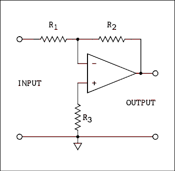
Figure 0.13, Inverting Amplifier with Op Amp.
For a verbal description click here.
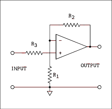
Figure 0.14, Noninverting Amplifier.
For a verbal description click here.
Figure 0.14 is the circuit of a noninverting amplifier. For this circuit the value of B is given byNoninverting Amplifier. B = R1 / (R1 + R2) (Eq. 0.30) This equation gives the value of B to be used in equation 0.26 or 0.27. For best temperature stability R3 should be equal to the parallel combination of R1 and R2.Power Supply.
The one thing that is missing from the two diagrams above are the power supply connections. Obviously the amplifier won't work without a source of power but it is assumed that those who are working with op amps know to connect a power supply.In most cases the power supply is symmetrical. For example plus 12 and minus 12 volts DC. This is often abbreviated +/- 12 V. If the writer is working with a sophisticated word processor the mathematical symbol with a plus sign above a minus sign will be used. There are some special op amps that have been designed to operate from a single supply but these are not often used. Also on rare occasions a designer may contrive to operate a symmetrical supply op amp from a single supply. This is generally not considered to be good engineering and is very rarely found in commercially manufactured equipment.
Back to Fun with Transistors.
Back to Fun with Tubes.
Back to Table of Contents.
Back to top.
0.7 FIELD EFFECT TRANSISTORS.
Junction FET.
A field effect transistor (FET) consist of a P-N junction on the side of a bar of silicon. The bar is known as the channel. One end of the channel is the Source, the other end is the Drain, and the other side of the P-N junction is the Gate. If the channel is N type semiconductor, the Gate is P type.When the P-N junction of the Gate and channel is reversed biased a depletion region in the channel reduces its effective cross section area. This restricts current flow between the Source and Drain. The larger the reverse bias, the more the channel is restricted and the smaller the current between Source and Drain. The JFET (Junction Field Effect Transistor) is almost never used with the Gate to channel junction forward biased.
Note: In oscillators and class C amplifiers the gate is purposefully driven positive which causes rectification. The rectified voltage is negative which provides proper bias for an N channel FET. When a MOSFET is used, see below, a diode is connected from Gate to Source to accomplish the necessary rectification.Metal Oxide Semiconductor FET (MOSFET).
Since the P-N junction is not normally forward biased, there is no need to have an actual P-N junction to create the depletion region. All that is needed is an electric field which can be created by a metallic plate. A small spot on the N type semiconductor is exposed to oxygen which creates a thin layer of silicon dioxide, hence the name. This thin glass layer is coated with metal which forms the gate. In operation an MOSFET acts almost the same as a JFET except that the gate can be driven positive for even higher conduction. Like its junction brother, the MOS FET is rarely operated in this condition. When used in an oscillator or a class C amplifier a diode is connected from Gate to Source to provide the necessary bias rectification. For convenience an N channel MOSFET is constructed on a P type substraight. This substraight is either internally connected to the Source, or is brought out to its own lead and the user must connect it to the most negative part of the circuit. This configuration is known as a depletion mode MOSFET.The MOSFET can be made in another configuration. A lightly doped P region, part of the substraight, is placed between the Source and Drain. This does not allow conduction between them. When the Gate is biased positively the holes in the region between Source and Drain are repelled deeper into the substraight leaving electrons behind. This effectively turns this region from P to N type semiconductor which allows conduction. The more positive the Gate the more conduction there is between Source and Drain. This is known as an enhancement mode MOSFET.
In 1987 MOSFETs were used primarily for switching in logic circuits. They are still used for that but a new generation of MOSFETs has been developed which will stand up to very high voltage and power. In that respect they are as close to silicon tubes as can be or probably ever will be achieved.
Back to Fun with Transistors.
Back to Fun with Tubes.
Back to Table of Contents.
Back to top.
0.8 FET Circuits.
The junction FET is used most often as a source follower, analogous to the emitter follower, for a high impedance input and a low impedance output. The input impedance is the resistor from gate to ground and the capacitance is a very few pf. The output impedance is 1 over the transductance in parallel with the source resistor.A special type of JFET known as a GASFET (Gallium Arsenide) is used as the low noise amplifier in satellite receivers.
High voltage MOSFETs are used in both analog and switching modes. The former includes but not limited to, * pass transistors in constant voltage and constant current power supplies, and output transistors in audio and servo amplifiers. The latter includes * switching power supplies, and variable speed drives for industrial electric motors.
* Have you ever read one of those terms of use things on the internet?Back to Fun with Transistors.
Back to Fun with Tubes.
Back to Table of Contents.
Back to top.
0.9 Vacuum Tube Fundamentals.
A vacuum tube is constructed inside a glass envelope which is evacuated to a very high level. The envelope is usually cylindrical which is the reason for the name. The internal structure is usually cylindrical as well. The filament or heater runs down the center. If the tube is a filamentary type it serves as the cathode which emits electrons when heated. If the tube is a heater/cathode type the cylindrical cathode surrounds the heater but is electrically insulated from it. Next out is the control grid. If there are additional grids they surround the control grid. Everything is surrounded by the plate or anode and is coaxial.Filament type tubes are the oldest type. In the golden age of tubes, 1950s, filament types were only used for very low power, used in portable radios, or high power, in radio transmitters. The heater/cathode type is by far the most common. They were used in radios, TV sets, audio amplifiers and a wide range of measurement and industrial equipment.
The minimum tube is a diode which consists of a cathode and anode. This is used primarily as a rectifier in power supplies and radio detectors.
Next higher is the triode, 3 element tube. (Note: The heater does not count when elements inside a tube are counted.) It consists of the cathode, control grid, and plate or anode. This type is favored by audio enthusiasts. Like the FET, the grid usually operates negative with respect to the cathode while the plate is positive.
Next higher on the totem pole is the tetrode which has two grids. The one closest to the cathode is the control grid and the outer one is known as the screen grid. The additional grid was added to serve as an electrostatic shield between the grid and plate. The control grid to plate capacitance caused RF amplifiers to oscillate and a means was needed to reduce this capacitance. The screen grid is made positive usually about equal to the plate or occasionally even higher. This type of tube has problems and very few true tetrodes were ever manufactured. There is a form of the tetrode in which a beam forming element was added between the screen grid and plate. It was connected to the cathode within the tube. This was done initially to avoid infringing on a patent but turned out to produce one of the best tubes ever made, the 6L6 and its many derivatives. The beam forming element suppressed secondary emission of electrons from the plate.
The pentode inserts a third grid between the screen grid and plate. This is also a method of suppressing secondary emission of electrons from the plate. It is called the suppressor grid. It is often brought out to a pin and the designer has to tie it to the cathode, or rarely, ground.
Toward the end of the golden age of tubes when there began to be significant competition from transistors, a type of tube was developed for use in car radios that would operate with no more than 12 volts on the plate. It was known as a space charge tube and was a pentode, but the control grid and screen grid were interchanged. The grid closest to the cathode was operated at 12 volts to get the electrons moving and the second grid was the control grid. The third grid served as a shield between the plate and control grid to prevent oscillation when the tube was used as a radio frequency amplifier.
Back to Fun with Transistors.
Back to Fun with Tubes.
Back to Table of Contents.
Back to top.
0.10 Tube Circuits.
The only circuits to be reviewed here are the resistance coupled amplifiers. Remember, this is only a refresher of knowledge you should already possess.
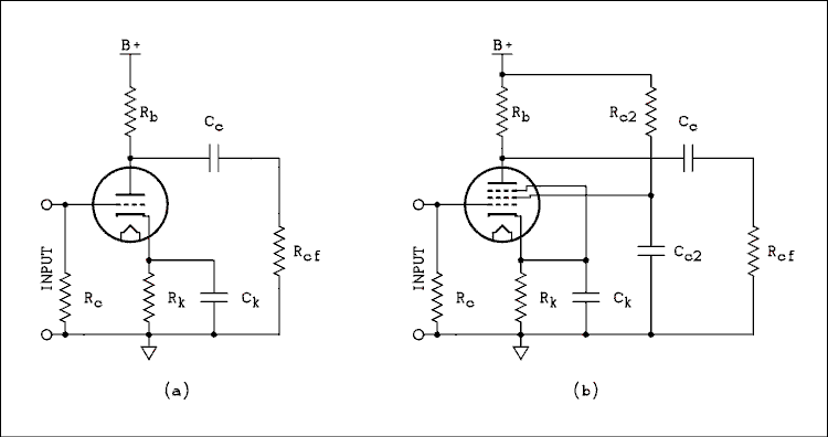
Figure 0.15 (a) Triode resistance coupled amplifier and (b) Pentode Resistance Coupled Amplifier.
For a verbal description click here.
The notation used is consistent with that used in resistance coupled amplifier tables found in the back of most tube manuals. The parts instead of being named for the elements they connect to, such as Rg and Rp use the name of the batteries that used to supply voltages to these elements. This dates back to the earliest years of vacuum tubes. Negative bias on the grid was once supplied by a C battery so the grid resistor is Rc. The plate supply battery was the B battery so the plate resistor is Rb. Voltage and current values are similarly subscripted. There was no K battery. The cathode resistor is Rk because C was already taken.Figure 0.15a is a triode resistance coupled amplifier. The current flowing through Rk produces a voltage drop which makes the cathode positive with respect to ground. The grid is held at ground potential by Rc so the grid is negative with respect to the cathode. This is an audio frequency amplifier. Ck filters the AC component from the cathode voltage which if present would reduce the gain of the amplifier. Note: Sometimes Ck is deliberately omitted which reduces distortion along with reducing the gain.
The output of this amplifier circuit appears across Rcf. Rcf is the grid resistor of the following stage. It is assumed that this amplifier stage is sending its signal to another amplifier stage.
Figure 0.15b is a pentode amplifier stage. Pentode circuits give higher gain than triodes but have a higher parts count. Biasing works the same way as in the triode circuit. Cc2 prevents reduction of the gain which would occur if AC signals were allowed to appear at the screen grid. This capacitor is never omitted. However, if the cathode bypass capacitor is omitted the screen grid bypass capacitor must be returned to the cathode instead of ground. Gain is higher and distortion lower than with Cc2 returned to ground.
Back to Fun with Transistors.
Back to Fun with Tubes.
Back to Table of Contents.
Back to top.