So, how was the core memory working?
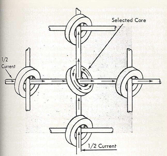
The cores were put at the intersection of rows and columns of a matrix of wires; there were two perpendicular wires going through each core.
The magnetic field of the core could be modified if each of the wires crossing in it was fed with a half current, for the sum of these two half currents was making a full current which was allowing the magnetic field of that core to be modified.
On the other hand, if only one wire was fed with a half current and not the other one, this half current alone was not enough to change the magnetic field of the core.
On the schema which is shown, only the central core is crossed with two wires fed with a half current, and it is the only one which will have its magnetic field modified.
The other cores have only one wire fed with a half current and the other wire has no current going through it, so their magnetic field will not be modified.
This process allows to specifically target the core which is to be modified (or read).
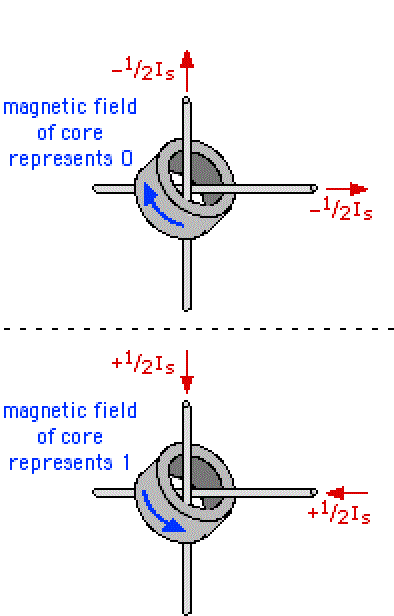
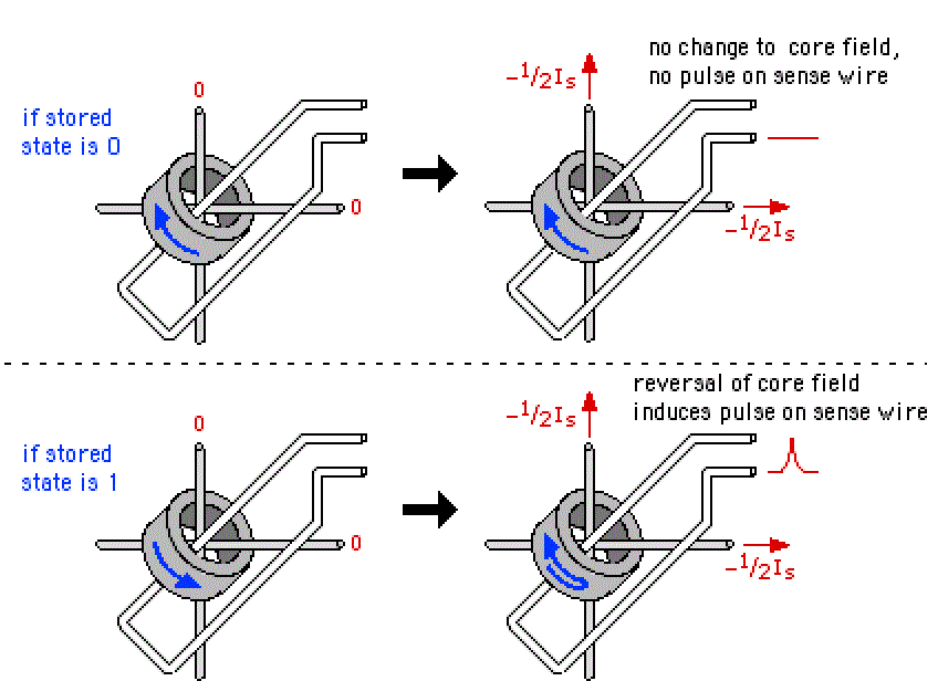
When the two crossing wires are fed with a negative current, the ferrite core is polarized negatively, and conversely, when the two crossing wires are fed with a positive current, the ferrite core is polarized positively.
The fact that the ferrite core is polarized negatively corresponds to a bit set to zero, and the fact that it is polarized positively corresponds to a bit set to one.

When the core is already polarized negatively, and negative currents are sent through the crossing wires, the magnetic field of the core will remain unchanged; a sense wire which goes through the core will then detect nothing; the computer then knows that a zero was stored on this core.
On the other hand, when the core is currently polarized positively and negative currents are sent through the crossing wires, the magnetic field of the ferrite core will change, and this change creates a short pulse through the sense wire; though this pulse is very short, the electronics is fast enough to detect it; it is the detection of this pulse which says that the ferrite core was polarized positively before the currents were sent through the wires; the computer then knows that a one was stored in this core.
The problem of the reading is that it is always made by sending a negative current through the crossing wires, and thence the core will always be polarized negatively after it has been read, even if it was polarized positively previous to the reading; that means that, if a pulse has been detected in the sense wire, positive currents must then be sent through the crossing wires so that the core returns to it previous state corresponding to the one it was memorizing (otherwise, next time a zero would be read instead of a one).
If may seem a little complicated explained that way, but in fact this process is extremely fast and allows to read the memory with a quite high speed.

So the cores are inserted into an array of wires, and these wires are commanded with circuits of which the schema is represented on the right; this circuit can send either a negative current (for reading the cores) or a positive current (for reprogramming the ones of the cores which have been detected to a one); the negative or positive current will only be sent if an enable signal allows it; this enable signal depends on the current memory address which is to be read or rewritten.
So, you can see that the principle of the core memory lays on a dynamic change of the magnetic field.
When the core memory is switched off, it is always deprogrammed, and cannot hold information; when it is switched on, the cores must first initially be polarized positively or negatively by sending either positive or negative currents, according to the fact that the cores must memorize a one or a zero.
And when a memory data is to be modified, the crossing wires of the cores corresponding to the ones of this data must be fed with positive currents (unless they already were positively polarized), and conversely the crossing wires of the cores corresponding to the zeroes of this data must be fed with negative currents (unless they already were negatively polarized).

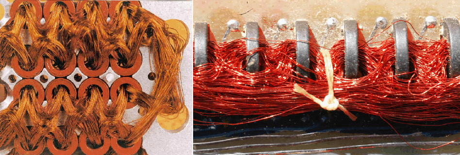
In the normal core memory, you can see that the activation wires passing through the cores have a quite important diameter relatively to the core.
Indeed, they must be able to carry a sufficient current to change the magnetic field of the core, and, if they were too thin, they would not be able to stand this current.
In the Wikipedia's article, they say that each half current was between 0.4 and 0.8 ampere (two half currents must be sent to change the magnetic field of the core, one is not enough); if it is a single wire which must change the magnetic field of the core, this current must be doubled; it would then be between 0.8 and 1.6 ampere.
Concerning the sense wires, they can be thinner, for the pulse they get is relatively weak.
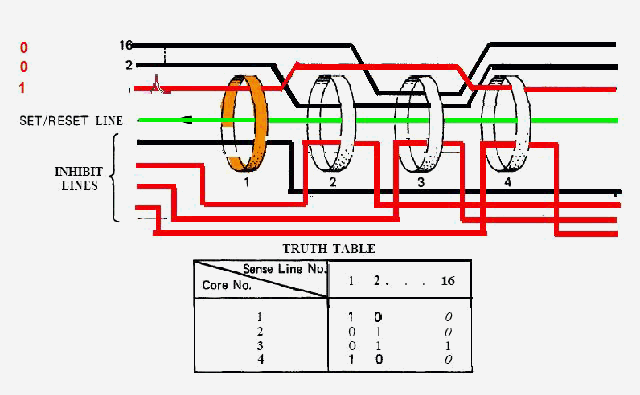
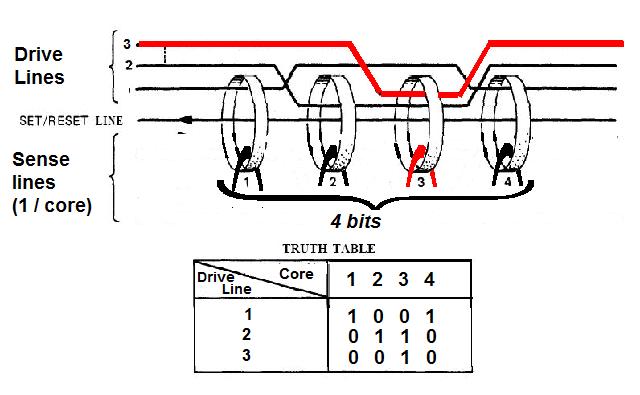
So, how was the "rope core memory" of Apollo working?
They were making the sense wires go through cores or over them; when a sense wire was going through a core, it was supposed to represent a one, and when it was going over instead of going through, it was supposed to represent a zero!
Up to 64 sense wires could go through a core!
I have found a documentation on the site of the NASA explaining how the core rope memory of Apollo and the erasable memory too were working.

First I have to give some explanation about the diode and the transistor, for I'll refer to these explanations in what follows.
A diode is a device which lets the current pass into one direction and blocks it in the other direction; and in the direction it lets the current pass, the diode behaves like a resistor of almost null value.
A transistor is a more sophisticated device which has three electrodes called the base (the electrode on the left), the emitter (the electrode with an arrow) and the collector (the top one).
The particularity of a transistor is that a small variation between the base and the emitted yields a bigger variation between the collector and the emitter; this particularity allows to use the transistor as an amplifier.
A transistor can also be used to block or allow a current between the collector and the emitter with a command inputted on the base of the transistor.
There are two types of transistors:
- In the transistors called "NPN" the current goes from the collector to emitter; these transistors are represented with the arrow of the emitter oriented toward the exterior of the transistor.
- In the transistors called "PNP" the current goes from the emitter to the collector; these transistors are represented with the arrow of the emitter oriented toward the interior of the transistor.
When the transistor is connected so that a current can go from the base to the emitter, the current can go from the collector to the emitter (or from the emitter to the collector in the case of a PNP); the transistor if then unblocked.
But, when the transistor is connected so that no current can go from the base to the emitter, the current cannot go from the commector to the emitter (or vice versa in the case of a PNP); the transistor is then blocked.
Now this is the the simplified schematics they give for explaining how the core rope memory of Apollo works.
In order to test which cores a sense line is passing through, and which cores it is bypassing, it is not possible to activate several cores in the same time.
Indeed, if two cores a sense line is passing through are activated simultaneously, the sense line will receive a pulse, but it will not be possible to know if the sense line is going through the first of these two cores, or the second one, or both, because, whether only the first core generates a pulse, or the second does, or both do, in all these cases the same pulse, standing for a 1, will be generated in the sense wire.
On the other hand, if the sense wire receives no pulse, then it can be sure that it is passing through none of these cores, and so that zeroes are programmed on these cores for this sense wire.
The only solution to test the bits on a sense line is to activate the cores one at a time (but when a core is activated, all the sense lines can simultaneously be tested for this core).
If the only the second core is activated, if a sense line sees a pulse, then it can be sure it is going through this core; and if it sees no pulse, it can be sure it is bypassing this core.
Likewise,if the only the third core is activated, if a sense line sees a pulse, then it can be sure it is going through this core; and if it sees no pulse, it can be sure it is bypassing this core.
When successively activating the second core and the third core, the second line receives a pulse in both cases, and it thence knows with certainly it has a 1 programmed on these two cores.

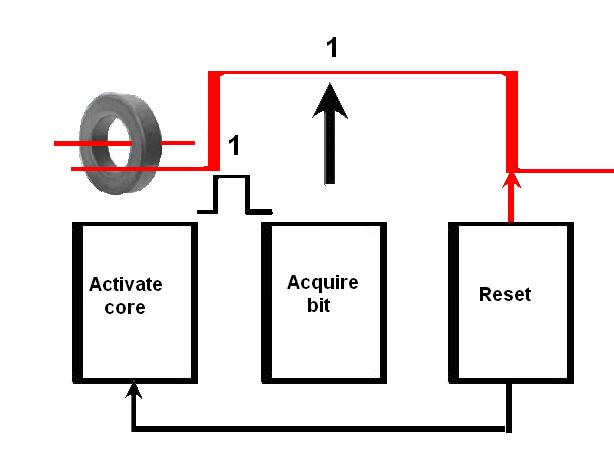
So, how to activate cores independently, so that only one can be activated at a time?
The most logical way is to make each activate line pass through a single core, one per core.
There are two possible ways:
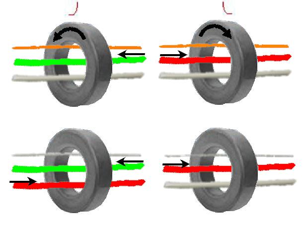
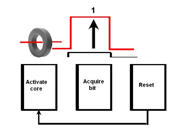
1) the way described on the upper half of the figure
A set current (left of the figure) in one direction is first sent into the activate line, changing the magnetic field of the core.
Then a reset current (right on the figure) in opposite direction is sent into the activate line to reset the magnetic field of the core back to its original state.
This double change of the magnetic field of the core generates a pulse into a sense line which goes through the core (and, if the sense line bypasses the core, it will see no pulse).
2) The way described on the lower half of the figure.
A set current (left of the figure) in one direction is first sent into the activate line, changing the magnetic field of the core.
Then a reset current (right on the figure) in opposite direction is sent, not into the activate line, but into a common reset line to reset the magnetic field of the core back to its original state.
This double change of the magnetic field of the core also generates a pulse into a sense line which goes through the core.
In this mode, only set currents are sent into the activate lines, and only the common reset line resets the cores.
But, curiously, they have not chosen this natural mode to activate the cores.
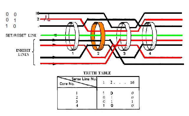
The lines which allow to select which core is activated are not "Activate lines", but "Inhibit lines", and they work in a converse way: They don't allow to activate a core, but to the contrary to prevent the activation of a core.
On my examples, the bottom wire going through a core is an inhibit line, the central wire is a common set/reset line which goes through all the cores, and the upper thinner wire is a sense wire.
1) The processus of activation of a core is described on the upper half of the figure.
A set current (left of the figure) in one direction is first sent into the common set/reset line, changing the magnetic field of the core.
Then a reset current (right on the figure) in opposite direction is sent into the common set/reset line, resetting the magnetic field of the core back to its original state.
This double change of the magnetic field of the core generates a pulse into a sense line which goes through the core (and, if the sense line bypasses the core, it will see no pulse).
2) in case that a core must not be activated because it is not currently the tested core, the processus of inhibition of the activation of the core is described on the lower half of the figure.
The set current (left of the figure) in one direction is sent into the common set/reset line, but a reset current in opposite direction is simultaneously sent into an inhibit line going through the core.
The set current and the reset current are of equal intensity, and, as they are opposed to each other, they are going to cancel each other; because of the reset current going through the inhibit line, the set current of the common set/reset line cannot change the magnetic field of the core, and thence no pulse will be generated by this core in a sense line passing through this core.
The reset current (right on the figure) is then sent into the common set/reset line, but, as the magnetic field has not been changed because of the inhibition, the core will not react to this reset.
So, in order to activate a single core, no current must be sent into the inhibit line(s) passing through this core, and, in all the other cores, there must be (at least) an inhibit line that a reset current is passing through.
(note too that the fact that currents are sent into two wires must not be compared with the currents sent into two wires in the normal core memory: In the normal core memory, it is two half currents complementing each other, and here it is two full currents cancelling each other).
So, the concept of the inhibit lines seems less obvious to use than the one of the activation lines, but it seems to work anyway.
Yet this concept creates big problems that we are going to see.
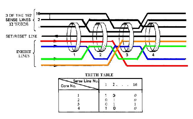
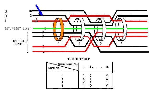
I have colored with different colors the four inhibit lines which allow to select or inhibit the cores.
You can see that each of these inhibit lines goes through two cores.
The third activation line goes through the second and fourth cores.
If a reset current is sent into this line only, the set current going through the common set/reset line will activate the first and third cores, for only the second and fourth are inhibited from changing the magnetic field of the core.
If we want only the first core to be activated, then reset currents must be sent both through the third and fourth inhibit lines.
Notice that these lines both go through the fourth core; that means that two reset currents instead of one will be sent through this core.
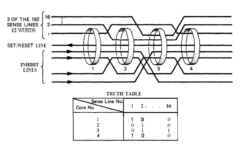
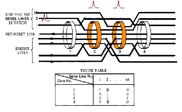
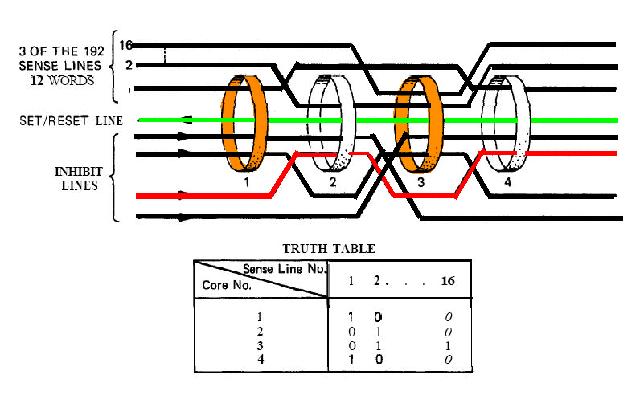
The process of reading of the bits programmed on the cores for the 16 sense lines is described in this demonstration.
Reset currents are first sent into the third and fourth inhibit lines when the set current is sent into the common set/reset line so that only the first core is activated.
As only the first sense line is going through the first core, but neither the second sense line nor the 16th sense line (the other sense lines are not specified), only the first sense line has a 1 programmed on this core while the other sense lines have a 0 programmed on this core.
So, for the first core, we have the combination "10...0" (starting from the first sense line).
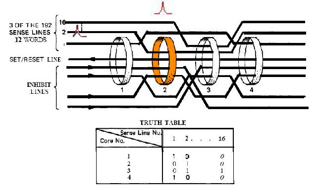
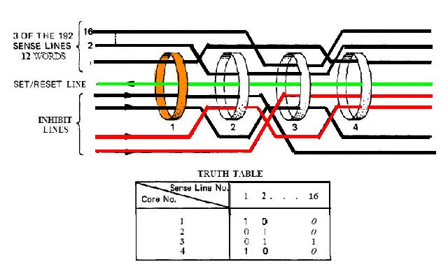
Then a reset current is sent through the second and fourth inhibit lines, causing the inhibition of all the cores save the second one, which is the currently tested one.
As only the second sense line is going through the second core, it is the only one which will get a pulse.
So, for the second core, we have the combination "01...0".

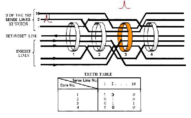
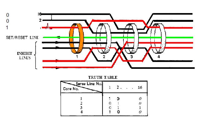
Then a reset current is sent through the first and third inhibit lines, causing the inhibition of all the cores save the third one, which is the currently tested one.
As the second and 16th sense lines are going through the third core, it is these two ones which will get a pulse.
So, for the third core, we have the combination "01...1".
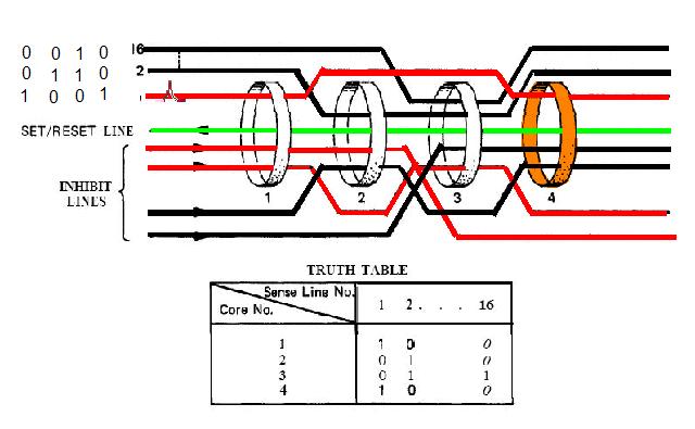
Then a reset current is sent through the first and second inhibit lines, causing the inhibition of all the cores save the fourth one, which is the currently tested one.
As only the first sense line is going through the fourth core, it is the only one which will get a pulse.
So, for the fourth core, we have the combination "10...0".
So, by successively activating one core at a time, it is possible to read the bits which have been programmed on the sense wires by making them either go through a core (for a 1) or bypass a core (for a 0).
With these 4 cores and 16 sense lines, it is possible to memorize 4*16=64 bits.
Notice however that we have had to send two reset currents at each step of the process (and that there is a core which receives two reset currents instead of one).

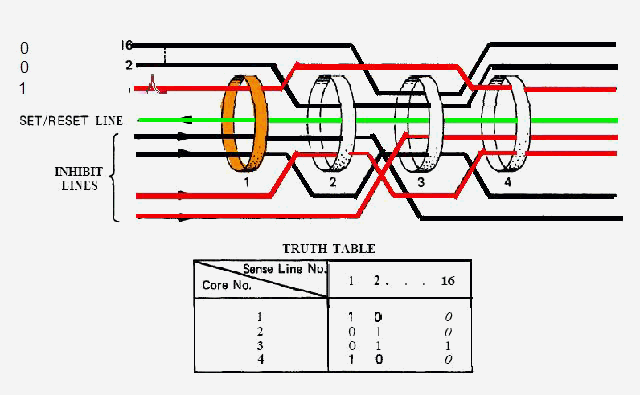
Another solution would be to make each inhibit line go through all the cores save one, so through 3 cores in this simplified example.
.The first inhibit line goes through the second, third and fourth cores, but not the first one; so sending a reset current into it will inhibit the activation of all the cores save the first one.
.The second inhibit line goes through the first, third and fourth cores, but not the second one; so sending a reset current into it will inhibit the activation of all the cores save the second one.
.The third inhibit line goes through the first, second, and fourth cores, but not the third one; so sending a reset current into it will inhibit the activation of all the cores save the third one.
.The fourth inhibit line goes through the first, second, and third cores, but not the fourth one; so sending a reset current into it will inhibit the activation of all the cores save the fourth one.
So now we just have to send one single inhibit current to test each core...but we have to make pass through each core a number of inhibit wires equal to the number of cores minus one (3 in our example of 4 cores).
We'll thence have to look for another solution.

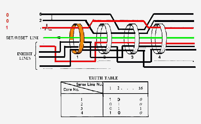
Another solution is to make pass a single inhibit line through each core:
. The first inhibit line will go only through the first core and will only allow to inhibit the first core.
. The second inhibit line will go only through the second core and will only allow to inhibit the second core.
...
So, in this solution, only one inhibit line goes through a core, and it solves the number of inhibit lines going through a core.
But, when a core is to be activated, all the other cores must be inhibited, which means that reset currents must be sent into all the inhibit lines save the inhibit lines going through the currently tested core.
Even if the management of the memory is made with separate units of which they show the schema, that still makes three currents which must be sent to read a core when one would have been enough if activate lines had been used instead of inhibit lines.

So, why not use the normal concept of "Activate wires" instead of "Inhibit wires"?
In the concept of "Activate wires", only one Set current is sent into an activate line when a core is tested, and only one activate line goes through a core.
No problem of multiple lines going through a core and no waste of energy.
This shows that using the concept of "Inhibit wires" to alternately activate the cores which are tested makes no sense, and that the concept of "activate lines" is the only reasonable concept which can work.
In fact, they could have activated the core which is to be tested the same way as in the conventional core memory: By sending half currents in lines and columns of a matrix of wires, so that the core which is tested is at the intersection of the line and column into which half currents are currently sent.

But the fact that they have illogically used "Inhibit lines" instead of "Activate lines" is not the only problem of the ROM card.
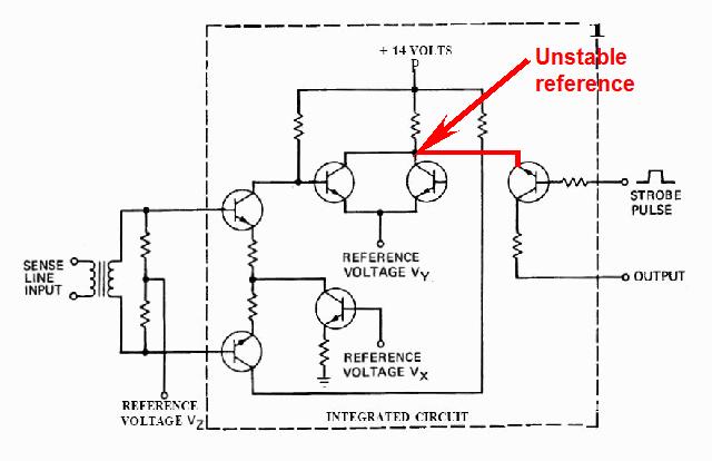
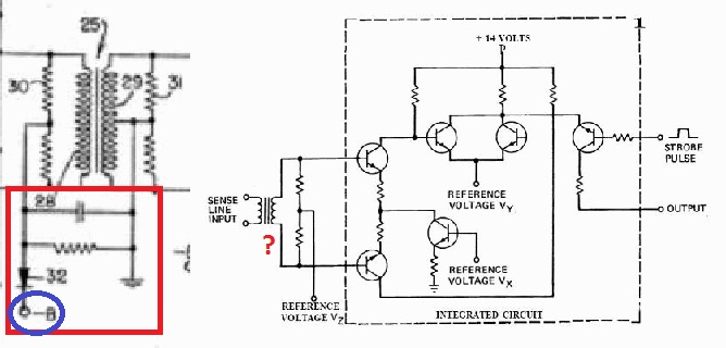
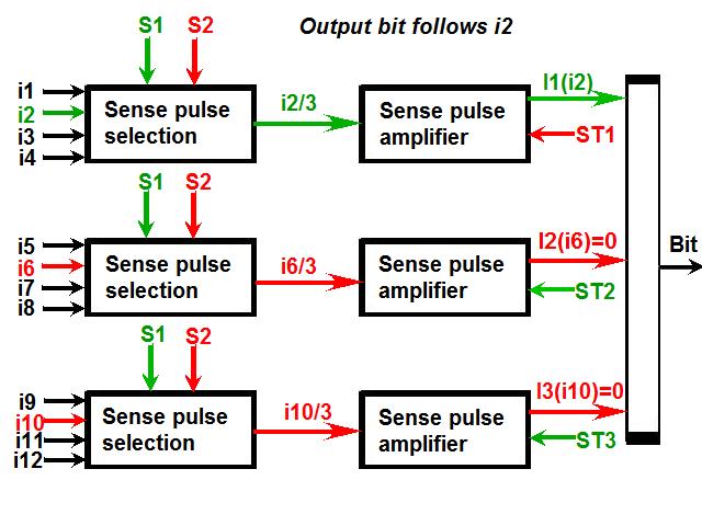
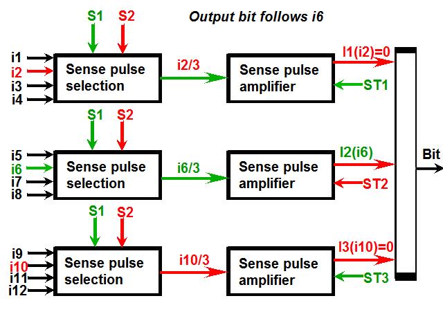
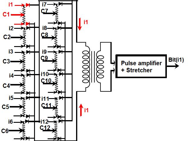
This schema shows how the pulse generated by the cores was read.
There were commands to activate the reading of the pulses generated by the cores individually.
In order to select the sense line which was to generate a pulse on the output coil (circled in blue), they were using line selection and module selection commands; for instance, on this schema, the only sense line of the four which can generate its pulse into the coil is the one framed in light green, because it is the only one connected to both a selected line (represented in dark green) and a selected module (also represented in dark green); the three other ones, framed in light red, cannot generate their pulse into the coil, for they are connected either to a non-selected line (represented in dark red) or a non-selected module (represented in dark red too), or even to both.
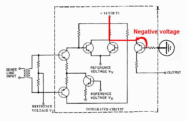
I give some explanations about the way the sense current was transmitted to the coil.
- I call VR the reference voltage of 14 Volts.
- I call R the value of the resistors
- I call I1 the intensity which comes from the line selection.
- I call I2 the intensity which goes through the diode D4 (which comes from the right).
- I call V the voltage of the common point I have circled in red.
The intensity which goes to the module selection point is equal to the sum of I1 and I2.
So V:
- Is equal to R*(I1+I2)
- Is also equal to VR-0.7-R*I1
- And also equal to VR-0.7-R*I2
(0.7 being the voltage between the ends of the diodes)
so we have the two equations:
R*(I1+I2)=VR-0.7-R*I1
R*(I1+I2)=VR-0.7-R*I2
Solving these equations gives:
I2=(VR-0.7)/(3*R)
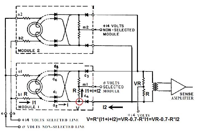
When the sense line generates a current I'll call i, this current also goes through the resistor which is connected to the module selection point.
So, now we have: V=R*(I1+i+I2)
And the equations become:
R*(I1+I2+i)=VR-0.7-R*I1
R*(I1+I2+i)=VR-0.7-R*I2
Solving this equation gives this result:
I2=(VR-0.7)/(3*R)-i/3
So a variation equal to i/3 relatively to the previous value.

That means that only one third of the very weak pulse in the sense line comes to the coil!
48 selected sense wires may potentially have a current going through, and, as the current of the selected sense wire is divided by three before coming to the primary of the coil of the amplifier, it makes a too weak current to be amplified.
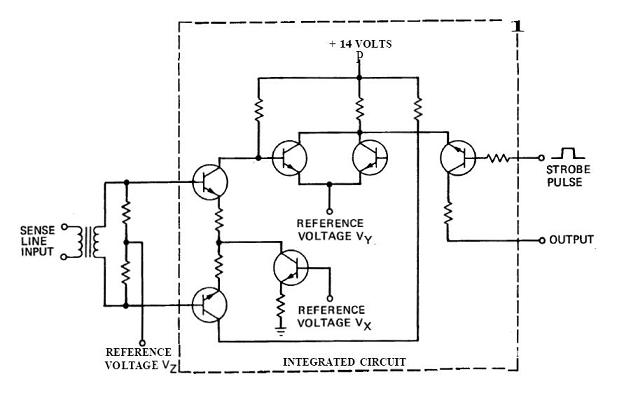
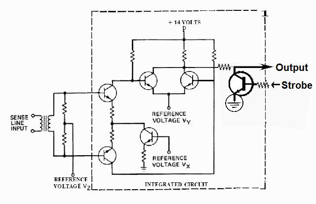
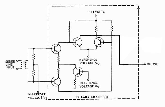
The pulse detected in the sense line is amplified to be used by a circuit of which the schematics is shown here.
We have seen that the pulse in the coil is only one third of the impulstion in the sense line.
Now we are going to see that this very weak pulse was even incorrectly amplified.

This amplifier uses two pairs of transistors; this special assembly is called a "push-pull"; it means that the first coupled pair of transistors (circled in green) amplifies the positive edge of the pulse (colored in green), and the second coupled pair of transistors (circled in blue) amplifies the other edge of the pulse (colored in blue).
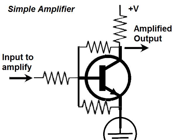
I show here a simple amplifier made with a transistor.
The signal to amplify is sent on the base of the transistor (the connection which is on the center of the transistor), and the amplified signal is obtained on the collector of the transistor.

On the first pair of the push-pull (transistors circled in green), the collector of the first transistor of the pair is connected on the base of the second transistor; it is the connection I have drawn in red.
But, on the second pair of the push-pull (transistors cicled in blue), the collector of the first transistor should also be connected to the base of the second transistor...but it is not the case, the connection between the collector of the first blue transistor and the base of the second blue transistor is missing; I have circled the place at which this missing connection should be visible...and is not.
As there is no connection between the two transistors of the second pair of the push-pull, it means that the second edge of the sense pulse cannot be amplified.
This omission is clearly intended as a clue of the fakery.

The missing connection between the base and the collector is certainly not accidental, for this mistake exists in two different schemas, one in a document dated 1966, and the other one dated 1972.
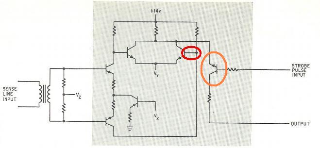
In an article published in 1967, Hopkins shows the schema of the amplifier, and, on this schema, the bug of the missing correction has been corrected; as the article of Hopkins has been published between the dates of the two documents in which the error exists, it shows that the argument that there might have been a decision of adding this connection or removing it does not hold.
Hopkins corrected this mistake to attract the attention, to show that something was abnormal.
However, Hopkins left the error of the incorrectly mounted output transistor.

About the incorrectly mounted output transistor, I initially thought that the strobe controlling the output was intended as an anomaly.
This would have been true on the prototype card, which had up to 64 sense wires passing through the cores.
Indeed, as there are 16 bits to simultaneously read, that would make 64/16=4 sense wires per bit.

As the sense line selection was allowing to select one in four sense lines, it then means that the selected sense line would have represented one bit of the 16 bits word to read.
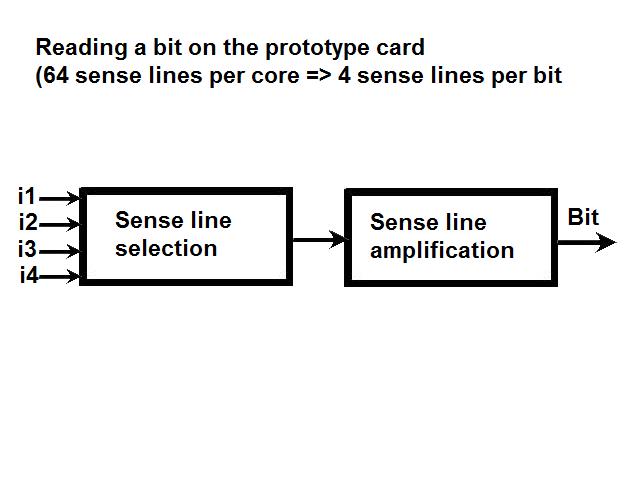
And the diagram to read a bit of the 16 bits word to read would have looked like this.
The sense line selection would have selected one of the four sense lines of the bit, the amplifier would have amplified it, and the output of the amplifier would directly have been a bit of the word.
So, for the prototype card, the strobe would indeed have been useless, and its presence an anomaly.
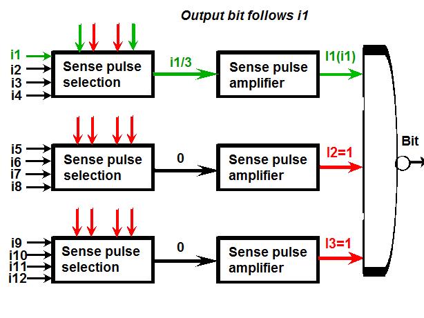
But, in the final core rope modules, it is not 64, but 192 wires which could pass through a core, three times more than for the prototype card.
That could make 192/16=12 sense lines for a bit.
It means that what the sense line selection was selecting was not representing a bit, but one in three possibilities for the bit.
For the sense line selection to select a sense line directly corresponding to a bit, it should have been able to select one in 12 lines.

Furthermore, as I have previously demonstrated, the sense line selection was reducing the current of the selected sense line to a third before it was coming to the amplifier.

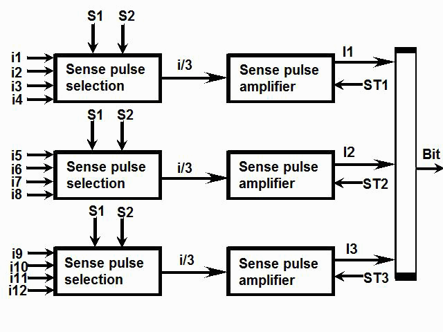
For the final core rope module, the diagram for the acquisition of a bit of the 16 bits word would have looked like this.
There would have been three sense line selection modules; each of these sense line selection modules would have selected one in 4 sense lines; each output of a sense line selection module would have come into an amplifier which would have amplified it, but only one amplifier's output would have been taken into account to represent the final bit, and the two other amplifier's outputs ignored, although they also were amplifying a selected sense line.
So, for the final core cope module, the strobe finally has a meaning: It was allowing to specify if this amplifier's output would be taken into account to represent the read bit, or ignored.
But, if the strobe is not finally an anomaly, the output transistor is still incorrectly connected.
It is in fact upside down.
When a NPN transistor (emitter's arrow oriented outward) is used to validate or invalidate a signal by controlling its base, its emitter is connected to a steady reference, generally the ground; here, it is not the case, for the emitter is connected to the amplifier stage's output, of which the voltage changes when it amplifies a pulse.
And, when the transistor's base would be grounded, and the amplifier's stage was not ampliying a pulse, it would have a negative voltage relatively to the emitter connected to the +14V, and it is not good for the transistor.
This is the way the output transistor should have been connected, with its emitter connected to the ground.

When the base of the transistor is activated, the output transistor would conduct, forcing the collector to the ground, and the final amplifier's output would then not follow the output of the amplifier stage, which means that it would not be selected to output the bit.

And, when the base would be grounded, the transistor's collector would then follow the output of the amplifier stage, which means that it would then be selected to output the bit.
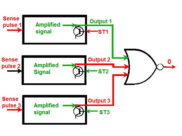
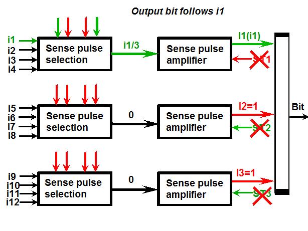
This simplified schema shows how the three amplifiers would be connected, so that only the output of one of them would be selected to output the bit.The outputs of the amplifiers would be inputted to a NOR gate; a NOR gate outputs a 1 when all its inputs are 0, and a 0 otherwise.
For two of the amplifiers, the ones which are not selected, the strobes would be activated, which would force their outputs to 0, and, for the third one, the one which is selected, the strobe would be grounded, allowing its output to follow the output of the amplifier's stage; when there is no pulse, this output would be 1, forcing the bit output to 0.

And, when a pulse would occur, the output of the amplifier's stage would be pulled down by the pulse, and the amplifier's output would become 0, which would force the output bit to 1.
So, if the missing connection between the base and the collector in the amplifier's stage is restored, and if the output transistor is correctly connected, does it mean that this amplifier would be correctly working?
In fact, there still is another problem, though it is less visible.
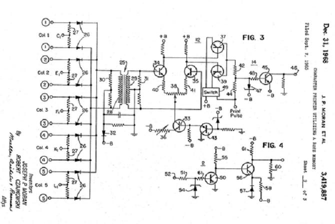
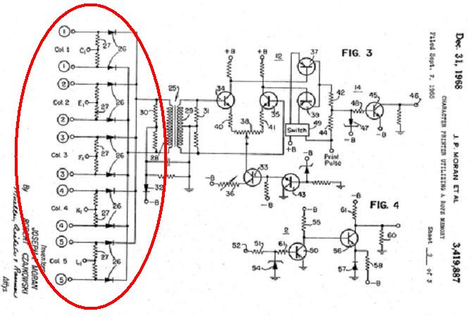
This is the schema of the selection of a sense line, and its amplification, in a patent of core rope memory of a printer, which memorizes the dot matrix for a character to be printed.
The cores, which represent lines of the dot matrix, are successively activated, and the sense lines, representing the columns of the dot matrix, are successively selected and amplified to print a dot of the character.
About this amplifier, the patent says that it does not only amplify the pulse, but also stretches it.
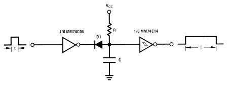
A pulse stretcher is an interface which allows to make a pulse longer, in order to exploit it more easily, to leave the time to read it.
Now, look: The part I have framed in red on printer's bit amplifier is called a RC circuit (with a resistor and a capacitor), and it allows to convert the pulse on the secondary of the transformer into a temporary permanent current, which then can be read by the reading logic.
After the bit was read, the state of the input I have circled in blue was changed, in order to discharge the capacitor, and allow the reading of the next bit.
In the AGC's bit amplifier, this circuit is absent, which means that the pulse is not memorized on the secondary of the transformer, and all the transformer does is to transmit the pulse to the amplifier without memorizing it, and, as such, it is useless.
If the pulse is not memorized, it cannot be read by the reading logic, for it passes too fast.

Now, why would the sense pulse need to be stretched?
For the bit interface to correctly acquire the bit from the sense pulse, there are two conditions:
1) The sense pulse must already be activated when it is read.
2) The sense pulse must still be activated when it is read.
If the bit was acquired exactly at the same time as the core is activated, it would not be acquired correctly for the sense pulse would not still be present.
That's why the process of the bit reading is made in three steps sequenced by timing:
1) Activation of the core
2) reading of the sense pulse
3) Reset

However, there is no guarantee that the pulse will still be active when the bit is acquired at the second step, in which case it would be read 0 whereas the pulse actually occurred.
That's why the pulse is stretched by the amplifier, so that the amplified pulse is certain to be present when it is acquired at the second step.
The reset at the third step cuts the stretched pulse moreover resetting the core.

So, how would the interface of a bit have worked, supposing all the flaws I showed would have allowed it to work?
There are 12 possible sense lines for a bit, but, for a given address, only one of these sense lines is to be taken into account.
Let's suppose the first one has to be taken into account to output the corresponding bit.
The first sense line selection module must select the first sense line; as the selection lines are inputted into the three selection modules, the two other selection modules also select the first line, but it is not relevant in fact, for their amplified outputs will not be taken into account.
The strobes are programmed so that it is the output of the first amplifier which is taken into account; finally the output bit corresponds to the first of the 12 sense lines associated with this bit.
Let's now suppose that it is the second of the 12 sense lines associated with the bit which is to represent the bit.
The first sense line selection module must now select its second input, and the strobes are still programmed so that it is the output of the first amplifier which is taken into account; finally the output bit corresponds to the second of the 12 sense lines associated with the bit.

Let's now suppose that it is the fifth of the 12 sense lines associated with the bit which is to represent the bit.
The second sense line selection module must select its first input, and the strobes must be programmed so that it is the output of the second amplifier which is taken into account; finally the output bit corresponds to the fifth of the 12 sense lines associated with the bit.
Let's now suppose that it is the sixth of the 12 sense lines associated wit the bit which is to represent the bit.
The second sense line selection module must select its second input, and the strobes must be programmed so that it is the output of the second amplifier which is taken into account; finally the output bit corresponds to the sixth of the 12 sense lines associated with the bit.

I don't think I have to give more examples: Selecting a sense line is done by making a double selection: selecting a sense line selection's input, and selecting an amplifier's output.
But, is this the best way for a bit's interface to work (ignoring the flaws of the amplifiers)?

I have only represented two commands to control the sense line selection block, for there only are four possible combinations to select one in four sense lines.
It means that each input is inputted twice in the control of the selection interface; once non inverted, and once inverted.
Now, it would be possible to control the sense line selection interface with four independent commands.
It would allow to select several sense lines in the sense time, which does not offer the least interest, but it would also allow to select none of them, which means that no current would go from the sense line selection interface to the corresponding amplifier, and this is more interesting on the other hand.
This might be interesting, for there would be no reason that a current would run through a sense line, and would be ampified, if the amplifier's output is not taken into account to generate the bit.
But, in this case, it would mean that the strobes would be unnecessary.
Indeed, since the corresponding amplifiers receive no pulse, their outputs will remain to 1, which means that the outputs of the amplifiers can directly be connected to a NAND gate, without being controlled by a strobe.
The amplifier which receives a pulse, will amplify it and will output a 0, which will force the NAND's output to a 1.
And, if the selected sense wire gets no pulse (i.e. does not pass through the activated core), the corresponding amplifier will output a 1, which will generate a 0 on the NAND's output, since the outputs of the other amplifiers remain to 1, as they receive no pulse, the output of their sense line selection interface being disabled.
In short, it means that, if the sense line selection interfaces could be controlled so that they would select no sense line at all, the strobe which controls the amplifier's output would become useless, and the amplifier could be simplified as I show.
But the strobe which controls the amplifier's output is here, and its presence proves that the engineers had excluded the possibility that the sense line selection interfaces could be controlled to select no sense line at all.
Now, let's consider again the selection and amplification of the sense lines of the printer's interface (and we can assume it has worked, it has not gone on the moon, it had no reason to cheat).
Look how the selection was done: the selection commands (C1 to C5) were inputtted on the middle of resistors bridges, and the sense lines were arriving on the extremities of these resistors bridges; they were connected to the primary of a transformer through diodes; a sense line was selected by activating its command line, while the other command lines were grounded; only the sense line of which the command line was activated had a current running through it, provided that it was going through the currently activated core, and it is its current which was running through the primary of the transformer, without being reduced, and amplified and stretched by the amplifier which follows.
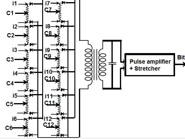
This printer's interface shows how the selection of the sense lines should have been made: There should have been an unique transformer, and as many resistors bridges as sense lines associated to the bit (12), as many command lines as sense lines to select; only one command would have been activated at a time, allowing a current to run through its associated sense line when it was passing through the activated core, and the current of the selected sense line would have run through the primary of the transformer without reduction; all the other 11 sense lines would not have had a current running through them, for their command lines would have been grounded; notice the capacitor connected on the secondary of the transformer, which allows to maintain the pulse after it has disappeared on the primary, and which leaves the time to read it; this capacitor is missing on the memory of Apollo.
For instance, if it is the first sense line which is to be read for the bit, only the first command line would be activated, and all the other ones grounded; the current of the first sense line would run through the transformer, entirely, without reduction, and would be correctly amplified and stretched by the unique amplifier of the bit, and the unique amplifier for the bit would have output a memorized bit, without a strobe being necessary.

And, likewise, if it is the second sense line which is to be read for the bit, only the second command line would be activated, and all the other ones grounded; the current of the second sense line would entirely run through the transformer, and would be correctly amplified and stretched by the unique amplifier of the bit.
So, this is definitively the way the bit's interface should have worked, provided that we keep the logic of using sense lines for programming the bits.
On one side, we have three sense line selection modules, reducing to a third the current of the selected sense line, and allowing three currents to run through three selected sense lines, three amplifiers, consuming currents, incorrectly amplifying the pulse, not stretching it, and incorrectly strobed, and, on the other side, we have an unique selected sense line, which is the only one which has a current passing through, which is not reduced before coming to the amplifier, which is correctly amplified and stretched by an unique amplifier which directly outputs the bit.
No use to tell you which is the best of the two; If you are not completely stupid, you must be able to figure out!

And selecting the sense line for the bit does not require more bits from the address bus for the improved interface than for the AGC interface.
Indeed, selecting the command among the 12 possible ones for the improved interface would be made with a circuit called "1 of N decoder"; it is a circuit which accepts a combination of n binary inputs and outputs 2^n outputs(Two n times multipled by itself), of which only one is activated at a time, which corresponds to the binary combination of the inputs; the displayed example shows how to validate one of the four outputs according to the binary combination of the two inputs.

Rather than showing a complete schema for a decoder having 4 inputs and 16 outputs, which would be a little overloaded to be legible, I show here an animation which shows how each gate of the decoder would be connected to the four inputs.
This decoder would allow to select one of the 12 commands of the improved bit interface from a 4 bit address.
It is not necessary to repeat this decoder for the 16 bits, the same decoder could be used for all the bit interfaces.
And concerning the bit interface of the AGC, a two bit address would be needed to select one sense line out of 4 ones, and another two bit address would be needed to select one of the three amplifier's outputs, which would also make a four bit address at total.
It means that the improved bit interface does not mean more bits to be controlled from the address bus than the AGC bit interface.

Moreover, the inhibit lines were not even used correctly; the way they were used, there were two inhibit currents passing through a core.

If they had been used correctly, then only one inhibit line would have passed through each core, and would have been activated to inhibit this core, like it was made in the printer's memory, which actually works.

Moreover the fact that the inhibition process is incorrect (because of two activated inhibit lines passing through a core), using the inhibit wires like it was made in the memory of Apollo also implies that the inhibit wires also had to be woven to alternately go through or bypass the cores.
And we are going to see that it complicates the weaving test.
Let's consider the sense wire 2, I indicated with a blue arrow.
This wire bypasses the first core (when it is correctly woven), because a 0 is programmed for this sense wire on the first core.
So, when a current is sent into the common set line (wire colored in green), and counter-currents are sent into the third and fourth inhibit lines, as these inhibit lines pass through all the cores save the first one, they will prevent all the cores from being activated by the current of the common set line, save the first core which will thus be the only one to be activated.
If the sense line 2 bypasses the first core, like it should, it will then show no current, showing that a 0 is programmed for this sense line on the first core; the detection of no current in the sense wire 2 will show it has been correctly woven.

Now, let's consider this situation.
The sense wire 2 (indicated with a blue arrow), instead of bypassing the first core, passes through it instead, because a gentle weaving hand has made a mistake.
The result is that, when the first core is activated (by sending a current into the common set line, and counter-currents into the third and fourth inhibit lines), it will show a current, when it should not.
The engineers will then deduce that a gentle weaving hand has made this sense wire pass through the first core, when it should have bypassed it, and will have the faulty sense wire removed and woven again.
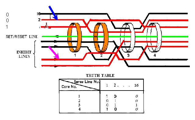
Now, let's consider this situation instead.
The sense wire 2 (indicated with a blue arrow) has been correctly woven, and bypasses the first core like it should.
But the third inhibit line (pointed by a pink arrow), instead of passing through the second core, bypasses it.
The result is that, when a current is sent through the common set line, and counter-currents through the third and fourth inhibit lines, there will be no activated inhibit line passing through the second core, and thence the second core will be activated in the same time as the first core, when it should not.
As the sense wire 2 passes through the second core, and that the second core is incorrectly activated, the sense wire 2 will be activated, not because the first core is activated, but because the second one is.
If the engineers think that the inhibit wires are correctly woven, they will deduce that the sense wire 2 has been incorrectly woven, that it passes through the first core when it should bypass it, and will have it rewoven, whereas it is correctly woven in fact, for it does bypass the first core, exactly like it should.
So reweaving the sense wire will not solve the situation.
So, does this mean that, if the bit interface had looked like this, it could have worked normally, and that it is the way it should have been conceived?
There is however a big difference with the printer's memory we have seen: In this printer's memory, the selection is made between all the sense lines which can pass through the cores; it means that there will never be more than one sense line that a current is passing through.
In this bit's interface, there is only one current passing through the selected sense line of the bit, but there are 16 bits to read for the word to be read, which means that there are 15 other currents which can run through the 15 other selected sense lines corresponding to the 15 other bits (provided of course that they go through the activated core, which can happen).
So, if this interface is used, it still means that there may be 16 currents running through selected sense lines (in the original interface of the AGC, it is 48), and 16 is too much, it implies a consistent reduction of current running into each of these selected sense lines (provided of course that they all go through the activated core, which may happen).
It means that, although this interface is much more performant than the one of the AGC, it still has a severe deficiency to work correctly.
That's why the core rope memories of other computers than the AGC, like the one of the UNIVAC (right on the stereoscopic view), although they show a similarity with the core rope memory of the AGC, work in a completely different way.

Indeed, in these memories, the lines, which pass through or bypass the cores, are not sense lines, but drive lines instead, and that changes everything.
In these memories, the cores have an unique sense wire.
Indeed, the text associated with this figure, in the patent of a core rope memory for a computer, is as follows:
"When the magnetic easy axis of the magnetic thin-film wire 1 is in the circumferential direction thereof, the magnetic thin-film wires 1 are used as information lines (which function doubly as digit lines and sense lines), and the conductor wires 2 are used as word drive lines."
In the memory of the AGC, only one core is activated at a time, and currents can go through several sense lines, and, in the core rope memories which actually work, only one drive line is activated at a time, and several cores may be activated by this drive line at a time, generating a current into each of their unique sense lines.

Instead of being read on an unique core, the bits are read on several cores.
With the same number of drive lines as sense lines, and the same number of cores, these memories can memorize the same number of bits, for, the same that a sense line programs a bit by passing through or bypassing a core, a drive line also programs a bit by passing through or bypassing a core.

So, if the core rope memory of the AGC was working according to the same principle as the core rope memories of other computers, which are proven to work, the schematics would be changed as I show here; the lines passing through or bypassing the cores would be labeled as drive lines, and not sense lines, and there would be no inhibit lines, which means that the latter would not have to be woven in the cores, unlike in the original memory of the AGC.

I explain here how it would work: The first drive line passes through the first and fourth cores, which means, that, when it is activated, the first and fourth cores would be activated, and their sense lines detecting a current, which would correspond to the four bit word 1001.

The second drive line passes through the second and third cores, which means, that, when it is activated, the second and third cores could be activated, and their sense lines detecting a current, which would correspond to the four bit word 0110.
Finally the third drive line passes through the third core, which means that, when it is activated, the third core could be activated, and its sense line detecting a current, which would correspond to the four bit word 0010.

This demonstration has been made with four cores, but the number of cores for reading a 16 bits word would in fact be extended to 16, in order to read the sixteen bits of the word.
So, you can see that this way of working is much better:
1) No need of inhibit lines
2) Only one current running into a sense line, which means that the current running through it would be consistent enough to be amplified.
So, this interface is much better than...
...this one, which itself is much better than...
...the one which has been conceived for the AGC.
This interface is so bad, it accumulates so many handicaps, that it has absolutely no chance to work, and the engineers knew it, for they wanted it to be extremely bad, and not to work.
This is the simplified schematics of the erasable memory.
The brick which is inside the loops of current represents the arrays of cores.
If no core rope memory has ever been used apart for Apollo (at least the way it was designed for Apollo), such is not the case of the normal erasable core memory which can perfectly work.
So, if the ROM memory of Apollo could not work, we could at least have expected that the RAM memory would have worked...But they have managed to make even the erasable memory not work!

I have represented in red the path of the write current; the current turns clockwise in the loop; this makes it go up in the block of the cores.

And I have represented in blue the path of the read current (the sense line); the current turns also clockwise, but, as it is on the left of the wite loop, this makes it go down in the block of the cores.

Now, what's abnormal is that the write current loop and the read current loop have a common part: it is the same wire which allows both to change the magnetic field of a core and also to sense the pulse which is generated by the change of magnetic field of a core.
This is absolutely impossible: The wire which allows to generate the change of magnetic field of the core by sending a current into it cannot also get the pulse generated by the change of the magnetic field; this change of magnetic field has to be detected in another wire, called sense wire; the wire generating the pulse and the one reading it cannot be the same, NO WAY!
And what makes it still more absurd is that the current of the write loop and the current of the read loop go in converse direction in their common part!
You might have thought that it was incoherent enough for the fakers to be satisfied?
Oh no, they had to add some more salt!
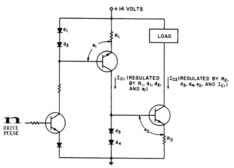
This is the schematics of the regulated pulse current driver which allows to read the sense pulse.

This interface contains two transistors (T2, T3) mounted in current regulator.
The current regulation is based on the fact that, when a current runs through a diode, it generates a difference of voltage of 0.7 volts on the ends of the diode.
When there is a pulse coming on the base of T1, T1 gets activated and the current can pass between the collector and the emitter of T1.
Because of the double diode connected to the base of T2, the voltage on the base of T2 is then equal to 14-1.4 volts (2x0.7=1.4); the voltage on the emitter of the PNP transistor T2 is equal to the voltage on the base of T2 plus 0.7 volts, so 14-0.7 volts; this would generate a regulated current of 0.7/R through the resistor R.
If T2 is activated, the current can go through its emitter to its collector, and also go through the double diode connected to the base of T3; the voltage on the base of T3 is then equal to 1.4 volts (2x0.7 volts).
If the transistor T2 is activated, the voltages on its emitter and its collector should be equal, but the double diodes D1&D2 force the voltage of the emitter to 13.3 volts, and the doubles diodes D3&D4 force the voltage of the collector to 1.4 volts!
It can't work, this interface is aberrant.
So, as incredible as it may seem, neither the ROM memory nor the RAM memory of Apollo could work.
They both appear as a complete joke.
But have no qualms for Apollo, Otto is here to manage the situation.

