Walkthrough - P ROMs
"I wanna live, I wanna love / But it's a long hard road, out of hell / You never said forever, could ever hurt like this" - "Long Hard Road Out Of Hell," Marilyn Manson
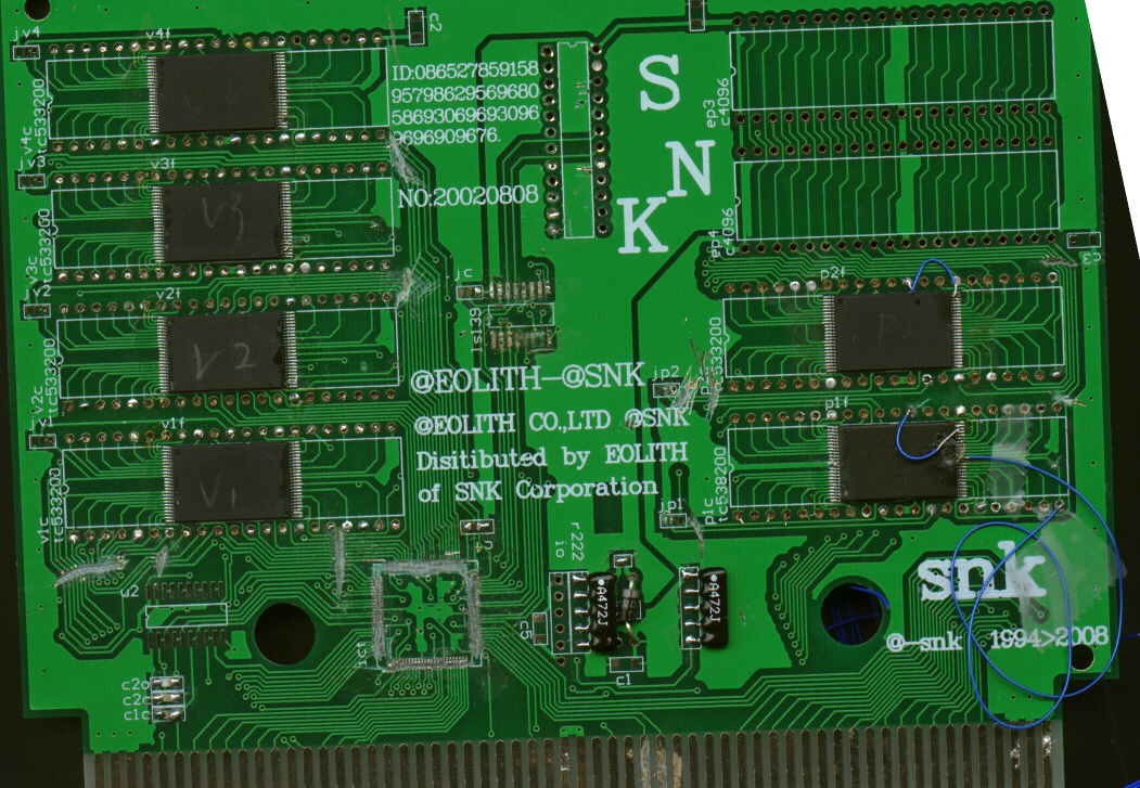
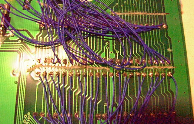
Now that you have seen what a smooth (if slightly more complicated than normal) dump is like, I will an example of a hellish (but doable) dump. On the KOF2K2 bootleg, the P ROMs were the hard part. I had one strike against me before I even started dumping: my P ROMs were physically damaged. This walkthrough will explain the entire process in detail and how I managed to overcome this problem. Here is a picture of the whole board with P ROMs (the two surface mounts on the right side of the board):
Since this was surface mount and I couldn't just remove the chips and read them (requires ALOT of skill to remove these chips without damaging them, and even worse, I would need to buy an expensive adapter to my ROM reader to read the surface mounts after taking them off), the first thing that crossed my mind was that I should try dumping this with the Neue Ziel. That would provide me with a P1 ROM with a minimal amount of effort. That attempt failed. Apparently, the banking scheme used on this bootleg was NOT the same as the banking schemes used for the old style boards, nor of the P1 of the encrypted boards. So I had to use a different, more direct approach.
First off, I had to identify the ROM. Now since this was a surface mount attached to where the normal P ROMs go, I could assume that the surface mounts could be read as normal P ROMs once I connected kynar wire from the solder holes on the board of where the normal P ROM dips would be stuck into to a socket that I could plug into my reader. However, I like to play it safe. I could make out a model number on the P ROMs. It is a bit difficult to see, but you can still see it on this scan:
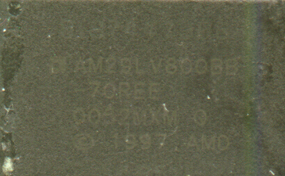
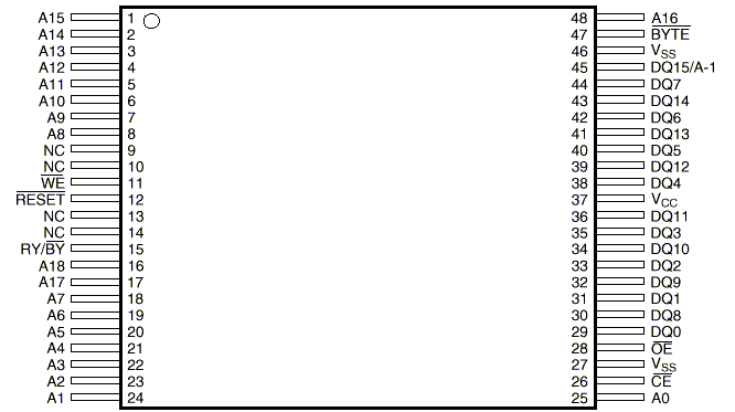
My next step was to look up the AM29LV800 chip. A quick search on Google led me to the datasheets for it. What I was most interested on that datasheet was the pin out diagram since that is what I would use to check for equivalency.
I compared that diagram with the pin out diagram of the M27C322, which is what I would use to read a normal P ROM.
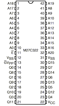
Using a multimeter, I placed one probe on the solder hole of the board where the pins of the normal ROM would go and then touched the corresponding pin of the surface mount. When I say corresponding pin, what I mean is that I would look at say pin 1 of the hole on the board and see that on a normal P ROM, that pin 1 would equal A18. I would then look on the diagram of the surface mount and see that A18 on that chip was pin 16. So pin 16 of the surface mount would correspond to pin 1 of the normal P ROM.
Everytime I did that, I got 0 resistance, which meant that all the pins were indeed mapped correctly and that I should be able to directly connect wires to the board and dump it. Click here to go back to the wiring section of the guide if you want to see a detailed explanation of wiring an adapter.
The two ROMs were wired together, so my first challenge was disabling the P2 ROM so that I could read the P1. Normally, this can be done by connecting output enable (pin 13 of the normal P ROM) of the P ROM you want disabled to VCC and the outout enable of the P ROM you want to read to GND. (Naturally, this means that on your adapter socket, pin 13 would have to remain unconnected. The ROM reader may say poor connection or some other error about pin 13, but since this is intentional, you can ignore those messages.) Unfortunately, doing that in this case didn't work. The data that I was getting out of P1 was a random garble that shifted dramatically with each read. I traced where everything was going on the P ROMs and found that they were connected to an Altera MAX logic chip. Since I couldn't figure out what the Altera MAX was doing (except for the fact that it was trying to ROM bank as I was trying to read the ROM, thus creating interference), I had no choice but to get rid of it. Notice the area a tad left to the bottom center of the board? See how it looks like something was ripped off of it? That's where that logic chip was. After removing that, I was still getting garble (still bad, but not quite as bad as before). I decided that it must be coming from the P2 and that I hadn't completely disabled it. After another attempt at making sure that the connections to the two pin 13s were good and still getting the same problems, I decided to sever the connections between the two P roms. You will notice severed connections near the P ROMs on that first picture. There were more connections on the other side, so I severed those as well.
Now when I read the data, I was getting constant data. I was elated. I quickly did a byteswap to see if I could find any recognizable text. (All NeoGeo P roms are byteswapped. So if you did a byteswap on it, you would be able to read the in game text like character names and winquotes. Many hex editors have the byteswap feature which will automatically flip the even and odd bytes for you.) I discovered that all my even columns produced good data, but the odd columns could be good or they could be bad. The data was constant, but I was getting severe typos in the odd columns. Basically, all characters were possibly 8 bytes greater than what they should be. So the character "A" would always be displayed as an "I." However, something that should be an "I" WAS an "I." This meant that anytime I saw an "I," I had no way of telling if it was supposed to be an "A" or if it really was an "I." The same problem existed for the P2 ROM. Clearly, this type of confused data (even though it was constant) would not do.
I noticed that whenever I dumped these P ROMs I would get an error complaining about pin 21 (data 11) being a poor connection. However, all multimeter tests showed that this connection was in fact good. Going on a hunch, I removed the wire going to pin 21 of the adapter. I then wired pin 21 of the adapter to VCC (used kynar wire to tie it together). I got the SAME data as before. I then moved pin 21 from VCC to GND. Just as I had expected, my errors were now REVERSED. Now all "I"s were displayed as "A"s, but if an "A" was supposed to be an "A" then it was still an "A." In other words, all my characters now had a possibility of being 8 bytes lesser than what they should be. Again, this only affected the odd columns. The even columns stayed constant and good.
This test confirmed what I was beginning to suspect: the data 11 connection between the surface mount and the solder hole was somehow faulty. I decided that maybe the problem was with the traces. So I physically connected pin 36 of the surface mount to pin 21 of the solder hole. As you can see in the first picture, that is why the bottom ROM (P1) has two wires coming out of it. The 2nd wire was this attempt at direct connection. Unfortunately, this failed to correct the problem and nothing changed. Since it failed, there was no point in repeating it with P2.
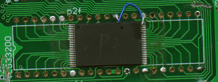
My next step was more drastic and required a bit of thinking outside the box. I noted that all the data in the even columns was good. The mistakes in the odd columns were constant, NOT random. So I would probably be safe in assuming that the data inside the odd columns was still good and that the problem was just with how it was being sent out. What if I could somehow force ALL the data to come out in even columns? I could then read the ROM twice, manually switching between even and odd bytes, but forcing them to ALL come through the even columns. Then all the data should be good since the ROM seems to have no problem sending data out through the even lines. Well, it turns out that there IS exactly such a way for this surface mount. By looking through the data sheets, I noted that it had something called bytemode (labeled BYTE with a line over it on the pin out). I did a quick multimeter test to confirm what I already knew: pin 47 (bytemode) was tied to pin 37 (VCC). This meant that the chip was ALWAYS in wordmode. A byte is 8 bits. A word is two bytes (16 bits). Since I was having a problem with data 11, that meant that I was OK on data lines 0-7 (the first or even byte) and that the only time I was getting messed up data was when I was trying to get the 2nd (odd) byte. By forcing the chip into bytemode, I could cause it to only send 8 bits of data at a time, thus ONLY using data 0-7 which I knew to be good. Data 11 could be left unused, and thus the problem of a damaged data line avoided altogether. However, this is easier said than done. First I had to gently flip up pin 47 so that it was no longer touching any traces on the board (thus disconnecting it from VCC) and then shorting it with GND. This is exactly what I did to both the P ROMs. In this picture, you can see it being done on P2. Pin 47 was bent up and there is a blue wire connecting that to pin 31 on the board. If you look at the pin outs, you will see that pin 31 on the board = VSS (which is the same as GND). (Note: In case you are wondering, NO, pin 47 is NOT shorted with pin 48. If you could see the board from another angle, it would be apparent that there is actually a gap between the exposed part of that wire and pin 48.)
After doing that, I manually banked between halves by switching pin 30 of my adapter between GND and VCC. The reason for doing that was that I noted that pin 30 of my adapter = pin 45 of the surface mount = data 15/a-1 which is the line used for switching between the two halves. I dumped the ROM twice, calling it p1a.rom and p1b.rom. This gave me two files with the odd bytes all blank. I then used the ROMWak utility to strip away the blankness and merge the two files.
romwak /b p1a.rom 1.rom
romwak /b p1b.rom 2.rom
romwak /m 1.rom 2.rom p1done.rom
I repeated this process with the P2 rom. Now I had data that was typo free and always constant, thus climbing my way out of this hell. It was quite a high, and I felt like partying like it was 1999. ;P BTW, there is an interesting followup lesson that should be learned from all this: NEVER EVER let the high of success get to you. It can make you do some really dumb things. I was so overjoyed at getting all the data that I forgot to cut away the last 3mb of repetitive data in P1. This mistake provided ammo for my critics and they used it as an opportunity for calling me incompetent. :-/
Quick recap:
Identifying the ROM
Checking for equivalency
Disabling P2
A serious problem
Avoiding the problem by using bytemode
Next Section:
Niue Ziel Theory
Go back to the table of contents

