Objective:
The aim of this
project is to realize a spectrum analyzer using analog circuits and a CRT
oscilloscope. This interface circuit will enable to use oscilloscopes as spectrum
analyzers.
Theory of
operation:
|
Fig. 1-The Spectrum analyzer block diagram |
The input signal is multiplied with the VCO (Voltage
controlled oscillator) output whose frequency is determined by the sawtooth generator. The
output is transmitted to the LPF (Low-Pass Filter) and it gives output when the input
frequency is equal to the VCO frequency. The output is given to the vertical plate of the
oscilloscope by an envelope detector.
The sawtooth generator drives the horizontal axis and the
voltage values of sawtooth signal correspond to the frequency axis of the spectrum
analyzer. Therefore we see a peak at the screen when the input frequencies are equal to
the VCO frequency.
Assume that the input frequency fx is constant
(for a pure sinusoidal) and the VCO frequency (fa) changes between 0 and fmax
and the value linearly depends on the voltage level of the sawtooth generator.
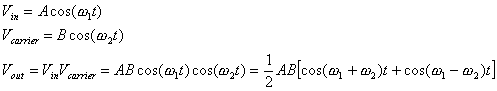
The output of the multiplier has the frequency components
fx + fa and fx – fa. Since the frequency of
the oscillator changes from 0 Hz to fmax, the LPF gives output when fx
= fa.
At the other frequencies of the VCO, the LPF gives no output so we can see a peak only at one point. The resolution depends on whether the LPF has a sharp cutoff. The frequency range of the input is determined by the minimum and the maximum frequencies that VCO can give. The envelope detector smoothes the LPF output.
Restrictions:
The input signal’s frequency should be constant during one period of the sawtooth signal in order the see the right number of peaks in the right position and the peak amplitude is proportional to the amplitude of the input signal.
If the input has more frequency components, the spectrum analyzer will also give peaks at the harmonic frequencies of the signal that are in the range of the VCO.
The amplitude of the input mustn’t be too high not to cause multiplier saturation.
The multiplier must have a bandwidth that is higher than the VCO frequency and it must perform double sideband suppressed carrier (DSB-SC) modulation to remove unwanted peak at DC level.
The envelope detector’s time constant must be smaller than the period of the filter output.
Design procedure:
Multiplier:
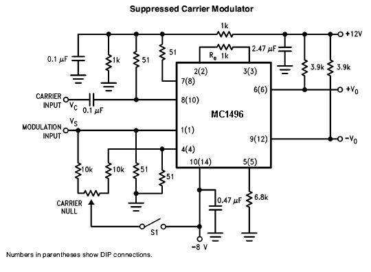
As a DSB-SC modulator we used Motorola MC1496.
|
Fig.2 - DSB-SC modulator (Taken from
Motorola MC1496 datasheet) |
The output of the multiplier includes the sum and difference of frequencies of VCO output and the input signal.
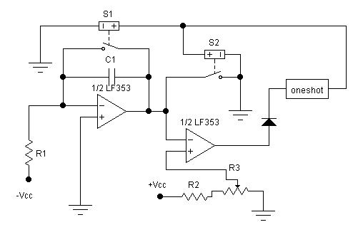
Sawtooth Signal Generator:
|
Fig. 3 - Schematic of sawtooth signal
generator |
The first op-amp is integrator, which integrates the DC signal, so the output is linearly increasing signal. Since the integrator is inverting and the input voltage is negative DC, the output is always positive. To make the sawtooth signal generator this linearly increasing signal should be reset at the desired level. This is done by the other components in the circuit.
The second op-amp is used as comparator. It determines the reset point of the sawtooth signal generator by the help of resistors R2 and R3. The output of the second op-amp is +Vcc or –Vcc according to the output voltage of the first op-amp.
Oneshot mono stable multivibrator is used to produce the pulse when the output voltage of the second op-amp is positive saturation. These pulses are used to trigger the switches. The switches are S1 and S2 are electronic switches in order to discharge capacitor when charged up to desired maximum of sawtooth signal. (Switches can be implemented by using 4066 CMOS IC). The maximum level of the sawtooth wave is determined by the voltage on R3.
The diode is used because the mono stable multivibrator is working at the positive signal level only.
The frequency of the sawtooth signal is determined by the capacitor C1, resistor R1 and input voltage of the first op-amp (-Vcc). Input voltage and the resistor R1 determine the current of the capacitor C1. If this current is changed the capacitor charge time is also changed and the frequency of the sawtooth signal is changed.
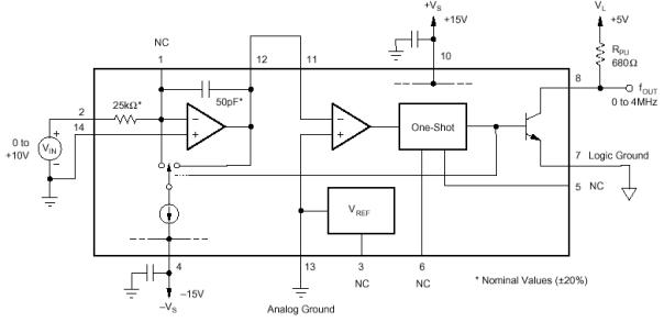
VCO:
The first VCO to be used was Burr-Brown’s VFC 110. It is selected because of the easiness in frequency band selection. The band can be changed by selecting appropriate values of resistors and capacitors from the table shown below.
|
Fig. 4a – VFC 110 simplified diagram
(taken from datasheet) |
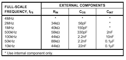
|
Fig.4b – Component selection table
(taken from datasheet) |
This IC isn’t used on the ongoing procedure because VFC 110 produces square wave output with different duty cycles. This means harmonic frequencies other than the fundamental will be observed in the oscilloscope screen. This helped us to improve the theory such that the VCO must produce sinusoidal waveform.
Instead of a square wave oscillator, we preferred sinusoidal oscillator but the design of variable frequency sinusoidal oscillator is difficult to realize. The best approach to sinusoidal oscillator is to create triangular waveforms and pass its output to a logarithmic wave-shaper. The triangle waveform can be easily obtained by integrating square wave. This algorithm also needs a variable oscillator. The use of the circuit given as sawtooth generator is enough to be used as a triangular generator when duty cycle is adjusted to 50 %.
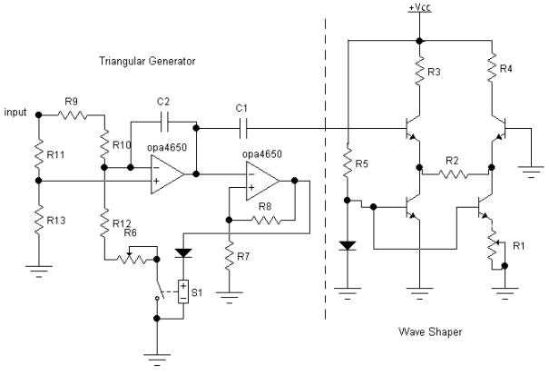
The sine-wave generator that is designed in this way is given in fig. 5. The op-amps used here can be anything that has the bandwidth greater than the operating frequency band.
|
Fig. 5 – Sine-wave generation by
using triangular generator and a wave shaper |
In this circuit the first op-amp is working as
integrator and the second op-amp is working as Schmitt trigger. The trigger voltages are
determined by the resistors R7 and R8. The input signal is applied between resistors R9
and R11. This signal determines the frequency of the triangular signal. In this circuit
configuration R11 and R13 is selected as equal. And the total of the resistors R9 and R10
should be twice the total of resistors R12 and R6. To analyze the circuit at constant
frequency let us consider constant input voltage is applied (let it say V). The voltage at
the positive terminal of the first op-amp is the half of the input voltage (R11=R13) and
because of the virtual ground the voltage at the negative terminal is also equal to V/2.
When switch S1 is open, the current that flows onto the capacitor C1 is equal to the ![]() . Because of this current, the output voltage of the first
op-amp increases in the positive level. When the output voltage of the first op-amp
reaches the voltage level that is determined by Schmitt trigger, the output voltage of the
Schmitt trigger changes polarity and become positive and because of that the electronic
switch S1 is closed. Since S1 connects the resistors R12 and R6 to the ground, current
flows onto this path. The current value is
. Because of this current, the output voltage of the first
op-amp increases in the positive level. When the output voltage of the first op-amp
reaches the voltage level that is determined by Schmitt trigger, the output voltage of the
Schmitt trigger changes polarity and become positive and because of that the electronic
switch S1 is closed. Since S1 connects the resistors R12 and R6 to the ground, current
flows onto this path. The current value is ![]() .
The current value at the path R9 and R10 does not change, it is the same (I). So the
current flows onto the capacitor C1 is reversed but at the same value and voltage on the
capacitor C1 decreases. The voltage at the output is limited by the voltage level of the
Schmitt trigger; when the output voltage of the first op-amp reaches the trigger level,
the output of the Schmitt trigger is changed and the S1 is opened. This procedure repeats.
The trimpot R6 is used to regulate the duty cycle of the triangular waveform. For 50 %
duty cycle, the following relation should be realized:
.
The current value at the path R9 and R10 does not change, it is the same (I). So the
current flows onto the capacitor C1 is reversed but at the same value and voltage on the
capacitor C1 decreases. The voltage at the output is limited by the voltage level of the
Schmitt trigger; when the output voltage of the first op-amp reaches the trigger level,
the output of the Schmitt trigger is changed and the S1 is opened. This procedure repeats.
The trimpot R6 is used to regulate the duty cycle of the triangular waveform. For 50 %
duty cycle, the following relation should be realized:
![]()
Triangular waveform is at the output of the first op-amp and the output of the second op-amp is square wave.
After this triangular waveform generator wave-shaper circuit is used to produce the sine wave from the triangular waveform. Two transistors at the bottom and the diode are working as the current source to bias the other transistors. The trimpot R2 is used to compensate the current level of the two transistors. Their current level should be equal. The current level is determined by resistor R5. Other two transistors are working as difference amplifier. But they don’t work at the linear region of the transistors; when the input signal level increases they start to working at the nonlinear region and the peak level of the input signal become flatten and triangular waveform looks like a sine wave. Capacitor C2 is used as ac coupler.
When the slowly varying input voltage is applied then the output of this circuit is FM modulated, its frequency change because of changing current onto the capacitor C1.the frequency of input voltage should be smaller than the minimum frequency of the triangular wave generator.
LPF:
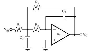
The most important part for good visualization and resolution is the low-pass filter. As the passband gets narrower, the peaks in the screen become sharper. LPF also brings out the restriction that the VCO starting frequency must be selected as much higher than the cutoff frequency of the LPF. Although the passband for a filter is defined as the frequency region that the power is half the maximum power, the passband in our project is defined as the frequency region that the output power is 1/10 of the maximum power output. The filter used herein is a type of 8th order MFB (Multiple Feedback) filter. The circuit consists of 4 cascaded
|
complex pole pair sections. The values of resistors, capacitors and cascade connections are determined with the help of a computer program called “Filter2” from Burr-Brown designed for MFB and Sallen-Key low-pass filter implementation. |
Fig. 6 – MFB
complex pole pair section |
|
The whole circuit is working as an analog spectrum analyzer properly but there is a restriction at the frequency of the sawtooth signal. When the sawtooth signal is at the minimum voltage level, the frequency of the VCO is at minimum value and when it is at maximum level, the frequency is maximum. So the time difference between minimum and maximum frequency value is T, where it is the period of the sawtooth signal. The time for 1Hz frequency change is
![]()
The minimum frequency difference that can be separated takes a time
![]() where BW is the minimum frequency
difference.
where BW is the minimum frequency
difference.
This time should be very larger than the period of the output signal of the LPF because at this time instant the output of the LPF should reach its stable point. The very large term can be thought as 10 times. So the final formula for the frequency of the sawtooth signal is as follows:
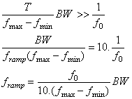
Where ![]() is
the cut-off frequency of the LPF and
is
the cut-off frequency of the LPF and ![]() is the frequency of the sawtooth signal.
is the frequency of the sawtooth signal. ![]() is the
frequency range of the VCO. If frequency range of the VCO is large and the cut-off
frequency of the LPF is small, then the frequency of the sawtooth signal is very small. To
see the frequency band of the input signal properly the oscilloscope with persistence
property can be used.
is the
frequency range of the VCO. If frequency range of the VCO is large and the cut-off
frequency of the LPF is small, then the frequency of the sawtooth signal is very small. To
see the frequency band of the input signal properly the oscilloscope with persistence
property can be used.
References:
1) Modern
Electrical Communications (Analog, Digital and Optical Systems) by Henry stark,
Franz B. Tuteur and John B. Anderson.
2) Motorola MC
1496 datasheet
3) Burr-Brown
VFC110 datasheet
4) AB-034 MFB
Filter Design, Application bulletin from Burr-Brown
Prepared by:
METİN AKTAŞ
HAKAN YESARİ GÜRSAN
with the help of