
I/O CARD
    - One analogue input to sample the tunneling current.
    - Four analogue outputs to drive the piezo quadrants.
    - 16-bit resolution.
    - Use of the parallel port for increased portability.
Eventually only two analogue outputs were used to control the piezo in two dimensions (X,Y). The Z position is controlled by the feedback circuit. Of the remaining two DACs, one is now used to provide the target tunnel current, Iref.
The latching nature of the parallel port makes it easy to carry the ttl-levels data bus to all the interface chips used. However the DAC712 chips need a 16-bit bus to operate. An extended bus is created by using an 8-bit latch to capture and hold the eight low order bits. Bus control is achieved using the other control lines of the parallel port.
For greater flexibility, it was decided to use the extra addressing capacity to provide for eight logic output lines and a fifth DAC. This DAC is conveniently being used to provide a programmable tip bias voltage. A cheaper option would be to use a few logic control lines to select from a handful of pre-set voltage levels. The logic lines connector also gives access to the four unused logic input lines that serve as control signals to the parallel port. So the logic port has four inputs and eight outputs.
Address decoding for the interface chips is provided using a 4515 binary decoder. It captures four bits off the data bus and activates one of sixteen chip-select lines. As there are less than eight devices to address, this function could have been achieved with an eight bit latch, capturing the full width of the data bus. This could provide the option of writing to all DACs simultaneously, as is required for instance, by the stick-slip function. This would also give the added benefit of limiting the chip variety. A small disadvantage is that more tracks would be needed to supply the whole byte bus to the chip. This is more significant if there are problems with board space. If, as happened, the confidence level in track etching is low, the tracks have to be made wider to compensate for this. A better way is to use a milling machine to provide thin tracks of consistent quality.
The analogue supply lines to the interface chips are driven by 7805 regulators. There is one for the DACs and a separate one for the ADC. There is provision, on board, to use an external 5V supply if required. This is done using 2.5mm power jacks. During noise reduction tests, this supply may be derived from a battery pack sitting close to the board.
Care has been taken to protect the rather expensive semiconductors on this card, and the parallel port itself. The resistors on the data bus, act as current limiters. This is important, in the unlikely event, that the software sets both the port and the iocard to output mode simultaneously. The output of the DACs is buffered by LM348 op-amps, whilst the logic outputs from the ADC are buffered using logic buffers. The ADC input was left intentionally unprotected in a bid to maintain sampling accuracy.
It is worth noting that in the original data sheets for the ADS7805P A/D converter, there is a tantalum capacitor connected the wrong way. This capacitor maintains the internal reference voltage, and a reverse polarity will cause the ADC to drift in a random manner.
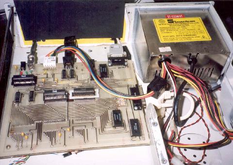
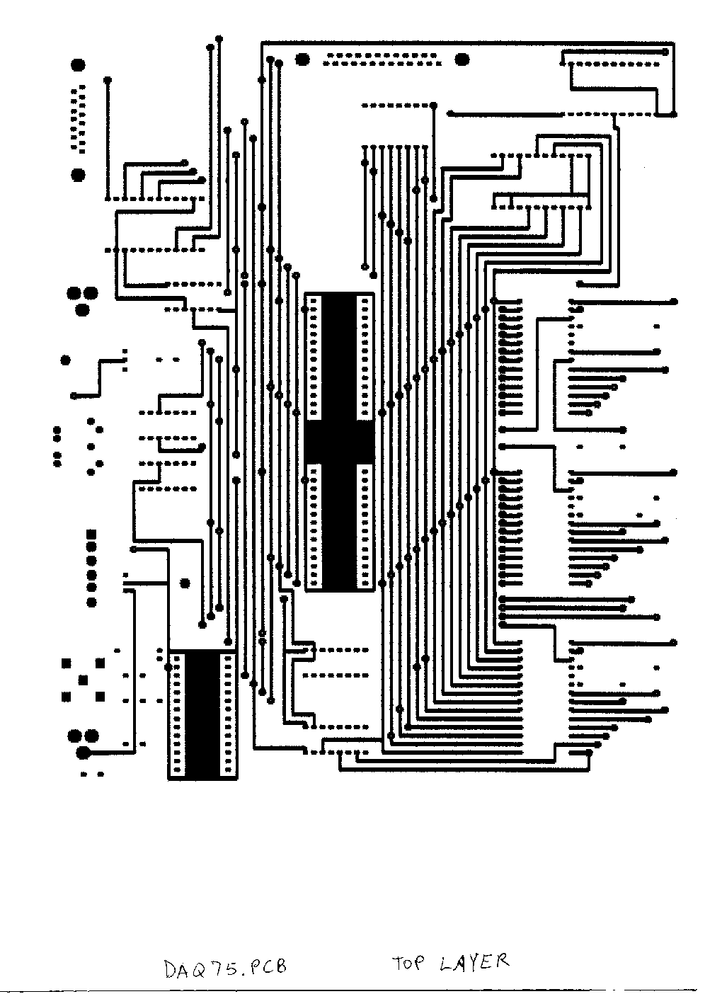
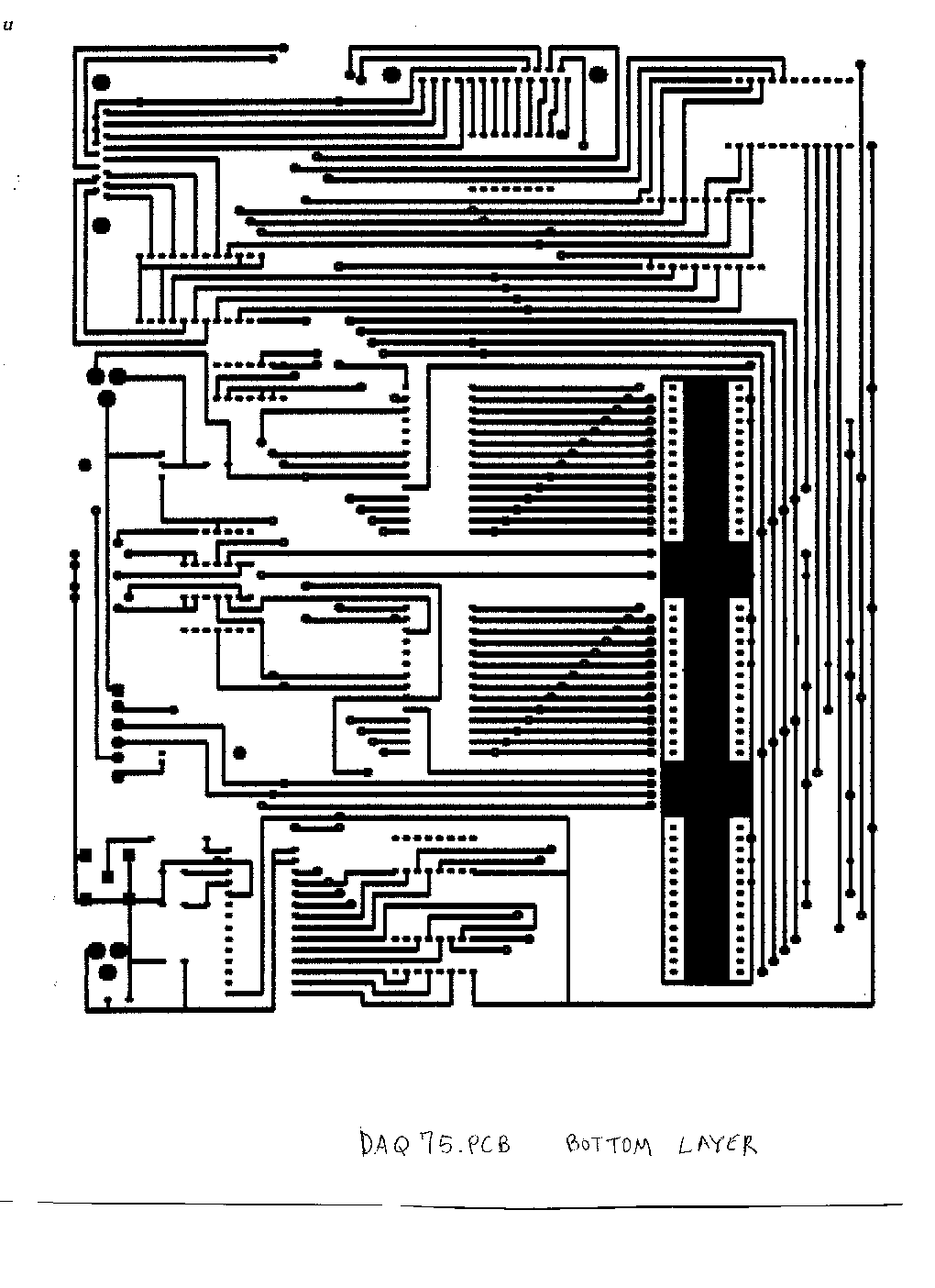
DO NOT USE PCB artwork (top) and PCB artwork (bottom) AS PRESENTED. The I/O chips actually have a narrower profile and will not fit. This was only realized after the board was constructed. These chips could only be used with the help of some home-made IC adapters, built specifically to patch up this mismatch. The full circuit details all the circuit connections following the topography of the pcb layout itself
The main power connector on the board is the same as in PC motherboards. This board was conveniently housed in an unused PC case and connected to a standard P.C. power supply.
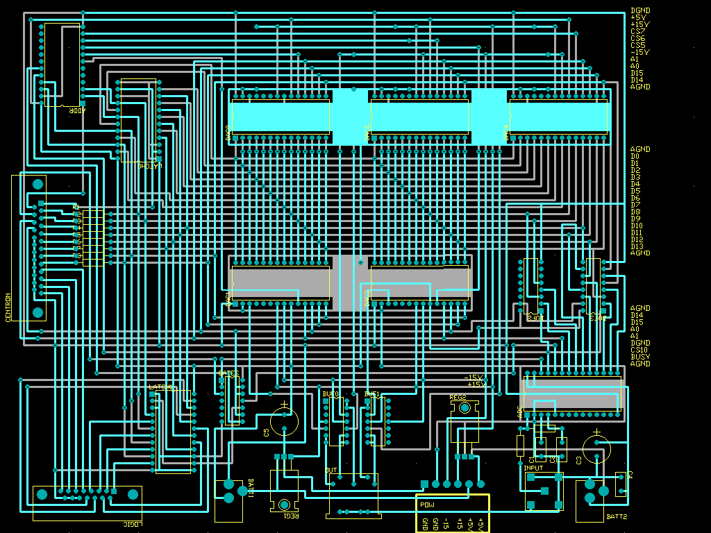
I/O card schematic C driver source
