
Slew Rate and t.i.d.
There appear to be different uses of the term 'slew rate'. I use it just to mean rate of change of voltage, but some use it to mean the maximum rate of change, which I refer to as 'maximum slew rate'. When maximum slew rate is specified the value given is invariably the 'large signal slew rate'. See the end of this page for an explanation of the difference between large-signal and small-signal slew rates.
A basic treatment of amplifier slew rate explaining how it is calculated is now added as a separate article: Slew Rate.
Many years ago Peter Baxandall published, in Wireless World, measurements of the slew rates of a range of high quality recorded music, from a range of sources, and found at that time that a power amplifier need only be capable of producing its full output swing undistorted up to 2 kHz to ensure it could give the maximum slew rate required by the music signals. In a 100 watt amplifier this represents a slew rate of about 0.5 V/µsec. A higher slew rate was needed in practice because of dust and scratches on vinyl records exciting tip-mass resonances. Unfiltered pilot tones from fm stereo radio and other unwanted non-music high frequency breakthrough were also found to increase the requirement.
These measurements were carried out before the advent of CDs, so I decided to repeat the Baxandall test using an identical differentiator circuit consisting of a 1n capacitor feeding a 1k resistor load. The output of a Marantz CD273SE was used. The output peaked at 2.5V, and the output across the 1k resistor was both calculated and checked with a sine wave source, the result being that the peak slew rate of a full level sine wave would give a peak output of 125mV at 8kHz, 156mV at 10kHz etc. The slew rate maximum observed by Baxandall would give an output of 31mV.
Checking a range of music CDs for a few hours it became apparent that a few recordings have maximum slew rate far greater than the Baxandall measurements. A small number of peaks around 120mV were found on some recordings, though most were much lower. The prize for greatest slew rate found goes to a single peak from 'Year 3000' by Busted, which hit 150mV, equivalent to the slew rate of a full level sine wave about 10kHz, i.e. five times greater than Baxandall's figure, and equivalent to a level of 2.5V/µsec for a 100W power level.An amplifier capable of close to full output at 8kHz should rarely if ever reach slew rate limiting with a good CD source, though Busted fans should aim for 10kHz. Any moderately well designed modern amplifier should of course have no problem exceeding this level by a very wide margin. My MJR7 for example was still happily producing its full output swing at the upper limit of my signal generator (100kHz) and should continue well beyond this. It is not possible to give a general specification of how far maximum amplifier slew rate needs to exceed the maximum music slew rate. Some amplifiers using heavy local feedback in the input stage still have low distortion at beyond 90% of their maximum slew rate, while others may be adding worse distortion at under 10% of their maximum slew rate. For these poorer circuits it may be easier in practice to improve input stage linearity rather than aim for an extremely high maximum slew rate. In either case the maximum slew rate alone tells us little if anything about how much an amplifier distorts music signals. A high specified value may in some cases indicate a bad choice of design priorities.
I have since found slew rate measurements for the newer DVD-A and SACD formats published by Stereophile. The maximum slew rate found was equivalent to that of a full level 12kHz sine-wave, so it appears that the maximum slew rates found are not much greater. No doubt there are a few higher slew rate values to be found, if anyone really wants to search for them, but my own tests suggest that even the 'high' values I found are rare isolated incidents of very short duration.
It is certainly possible to find faulty, or badly designed signal sources with interference pickup and other non-music high frequency components at a high level, but amplifying such a signal and applying it to your expensive speakers should definitely be avoided. Most high frequency speaker drivers use small light voice coils to extend the frequency response, and rely on the low average levels of high frequency energy in music to keep dissipation down to safe levels. Any excessive high frequency components should ideally be filtered out ahead of the power amplifier. If slew rate limiting occured this could actually reduce high frequency energy and help protect the speakers, but damage could be done well before this occurs. (Amplitude limiting can increase high frequency energy and make matters worse.)
Even if an unwanted high frequency signal is not at sufficient level to destroy a high frequency drive unit it will still cause an increase in its voice coil temperature, which will increase its resistance and cause a fall in sound level of the wanted signal, so high frequency signals well above 20kHz can certainly have an audible effect. Low pass filtering at the input will add some phase shift, but most of this will be equivalent to a constant, frequency independent time delay, and therefore inaudible. The additional unwanted phase error was analysed by Dr Leach, Differential Time-Delay Distortion who concluded that for a maximum phase error of only 5 degrees up to 20kHz a first-order low-pass filter -3dB frequency can be as low as 35kHz, and for a second-order Bessel filter it can be reduced to 25kHz, though the gain error may then become more important.
If amplifiers are to be tested with square waves close to the clipping level then to keep the slew rate down to the maximum level found in my CD tests the square wave must be passed through a low pass first order filter with its -3dB frequency at 5kHz. This gives the same maximum slew rate as a sine wave of the same peak level with frequency 10kHz.The DIM-100 test uses a square wave passed through a 100kHz filter, equivalent to the slew rate of a similar level 200kHz sine wave. Such tests may be to the advantage of designs with very high maximum slew rate, but have nothing to do with amplifying music from a good quality source.
TID
Another term, related to supposed slew rate problems, is 'transient intermodulation distortion', or t.i.d. which was a common concern at one time, and still inspires some designers to abandon overall negative feedback in the belief that doing so will protect against this particular affliction.
One of the early treatments of t.i.d. may be responsible for some of the misunderstandings. It was published as an appendix to an article by Daugherty and Greiner entitled 'Some Design Objectives for Audio Power Amplifiers' (March 1966, IEEE Transactions on Audio and Electroacoustics.) The incorrect conclusion of their analysis was that the 'open-loop response' of an amplifier using overall negative feedback should be at least 20kHz if this is the bandwidth of the signal source. This refers to the frequency at which the open loop gain falls by 3dB. An example was worked out to show that if this were not the case, then a step function applied via a 20kHz low-pass filter would produce an error signal with an overshoot at the input of the amplifier. It was shown in one example that although the error signal settled down eventually to a steady state level of 100mV the overshoot reached 527mV. This was described as a '427% momentary overload'. This is clearly an incorrect description. An overshoot is not the same thing as an overload. If the input stage is capable of remaining linear with the 527mV input, then there is no overload in this stage. If required such a stage can easily be designed using local negative feedback, though in practice such high error voltages should not occur in any reasonably well designed modern amplifier. (It is important to distinguish between 'error voltage' and non-linear distortion. The error voltage referred to in this case is just the total input stage differential input voltage, and may be primarily determined by open-loop gain, while distortion in the input stage will depend on the amplitude of the signal it is required to handle.)
A worse error, however, is merely to compare the overshoot amplitude to the steady state amplitude to give a percentage overshoot, and then state that the requirement to keep this percentage low will then keep distortion low also. Compare the two curves b and c in Fig.1. showing the voltage at the input of an amplifier input stage with a step signal applied.
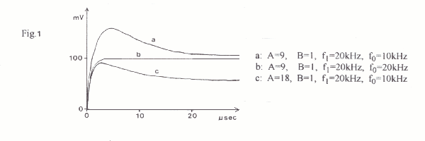
Curve b has no overshoot, but curve c has 58% overshoot relative to its final level, and yet it is curve b which has the greater amplitude, and will lead to the greater distortion in an amplifier stage. It is the maximum amplitude we must pay attention to, not the percentage overshoot relative to the eventual steady state level. The distortion produced by curve b will, however, not be associated with the transient any more than with the steady state signal, so in a sense we can say that there is no t.i.d. simply because the steady state distortion is at the same level as the transient distortion. Aiming to reduce t.i.d. irrespective of how this is achieved may in fact have the effect of increasing the steady state distortion to the point where the transient induced distortion is no longer distinguishable, which is almost certainly a bad idea.
To see the origins of the curves in Fig.1 look at the circuit in Fig.2:
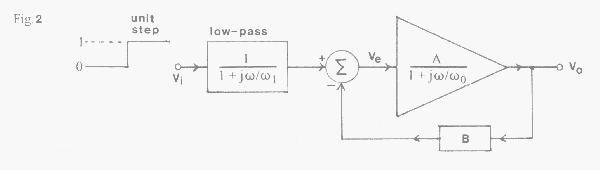
This shows a unit step function applied to a feedback amplifier via a first order low-pass filter with a response -3 dB at w1. The amplifier has open loop gain A at low frequencies, falling at 6dB per octave above w0. The gain of the feedback network is B, and the resulting error voltage at the input stage of the amplifier is Ve. For the unit step input the error voltage is given by the equation:
This function is plotted for three combinations of A, B, f1 and f0 in Fig.1. The frequencies in kHz are specified rather than the angular frequencies used in the equations, as these are more familiar to most of us. In all cases 100% overall fedback is applied, so B=1. The same input filter is used in all cases with -3dB at 20kHz. All we are varying are the open loop gain and frequency response of the amplifier, and the three different cases are plotted as straight-line approximations in Fig.3:
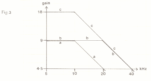
Response b is the commonly recommended 20kHz bandwidth to give zero t.i.d. and the other two responses are both -3dB at 10kHz, which we are often assured will lead to t.i.d. The reason why two such responses are shown can be seen by looking at one final diagram. Fig.4:
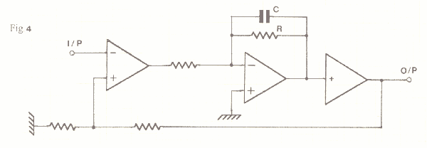
This is a commonly used configuration for a power amplifier. A differential input stage feeds an inverting driver stage which in turn feeds a unity gain output stage. The driver stage has local feedback via C and R which determine the open loop frequency response of the amplifier, and hopefully stabilise the overall feedback loop. Having chosen the minimum possible value of C to maintain stability we can then choose R to determine the -3dB open loop frequency response. Choosing R to give 20kHz bandwidth then gives result b in Figs 1 and 3. To reduce the open loop bandwidth to 10kHz we have a choice. We can increase either C or R. Increasing R by a factor of 2 gives result c, which gives the same open loop response at high frequencies as b, and therefore does not affect the stability to a great extent, yet it gives a peak error signal voltage reduced by 10% and twice as much negative feedback over most of the frequency range. Both transient and steady state distortion will be reduced, even though we have reduced the open loop frequency response to only half the value supposedly needed.
It is only if we instead increase C by a factor of 2 to reduce the bandwidth giving the results shown as 'a' that we find a 58% overshoot relative to the 100mV steady state error voltage, and we can truly say that transient induced distortion has been increased. But now C is much larger than is required for stability, and there is no justification for the increase. It is only the increase in R which is beneficial, and in general this can be omitted altogether and the open loop frequency response allowed to fall to under 100Hz, as is often done with op-amps, with no detrimental effects.
To summarise: the open-loop -3dB frequency is not the factor we need to worry about, any more than it is the percentage overshoot on the error voltage. What matters is to keep the maximum error voltage down to a level at which the input stage remains adequately linear. Some of the methods known to help achieve this are:
1). The input stage can be made more linear by the use of local feedback. This could involve using a complementary feedback pair instead of a single device, as in my own recent designs, or the addition of emitter degeneration resistors plus increased transistor current.
2). The high frequency compensation capacitor can be taken back to the input of the input stage rather than just applied to the driver stage so that increased current to drive this capacitor is not needed by the input stage. (This method was recommended by John Linsley Hood.)
3). The gain-bandwidth product can be increased. This is equivalent to reducing the high frequency compensation capacitor C in the diagram above. This may cause stability problems unless other changes are also made. Using a mosfet output stage generally makes possible a far higher gain-bandwidth product than for bjt output designs.
4). A low-pass filter at the amplifier input will reduce the possibility of excessive high frequency signal components causing problems.Whether high open-loop bandwidth ensures low TID depends on how the high bandwidth is achieved, but what about designing for high slew-rate, which some designers say is the way to avoid TID? Here there may be a more reliable link in that the sort of things we would do to increase the slew rate limit generally also have the effect of reducing TID. Here however there is still a potentially misleading aspect, because it is possible to reduce TID by improving input stage linearity, which can be done using local feedback in ways which have little effect on the slew rate limit, for example by replacing single devices with complementary feedback pairs. Saying that to reduce TID we must increase the slew rate limit is as wrong as saying we must increase the open-loop -3dB frequency.
The error of looking at the percentage overshoot and confusing this with overshoot amplitude in the Daugherty and Greiner article is surprisingly common. Maybe this has been repeatedly copied without adequate checks. For example, 'The Theory of Transient Intermodulation Distortion' by Otala and Lienonen from 1977 includes a graph, their Fig. 6, showing the ratio of overshoot amplitude to steady state amplitude, clearly marked as such on the vertical axis of the graph and described as such in the main text, yet the description below the diagram describes it as 'The maximum value Vmax of the overshoot', which it is certainly not, it is the ratio of two voltages. This is a crucial difference, to reduce the ratio of the two voltages the use of a high open-loop -3dB frequency is effective, but to reduce the actual peak voltage it is not necessarily effective depending on how it is achieved, as demonstrated above. The text then says that feedback over 40dB inevitably leads to rather large overshoots within the amplifier. My own mosfet amplifiers have about 80dB feedback at low to medium frequencies, but the overshoot from an input step function is well under 1mV at the input of the input stage.
Small Signal 'Slew Rate'
Large-signal maximum slew-rate is usually a non-linear input stage limiting effect, and the input signal amplitude needed to achieve this can be widely different for different input stage designs. Input stages using fets, or using bjts with emitter degeneration resistors, may need 1V or more differential input voltage to cause input stage limiting and achieve the maximum slew-rate specified. Used as a unity gain buffer for example, the difference between input and output voltages is equal to the input stage differential input, and should ideally be zero, but close to maximum slew-rate the difference could be around 1V, which is then an error voltage.
The actual output slew-rate achieved with a fast input step at a lower voltage may be far below the large-signal value. This is no longer a non-linear effect, but is determined by falling high frequency open-loop gain. A high value of maximum large-signal slew rate is no guarantee of a good small-signal value. Usually it is the gain-bandwidth product which determines the maximum small-signal output slew-rate.A good example of the difference between high and low level behaviour can be seen by looking at some typical op-amp specifications. The TL071 jfet op-amp has a maximum slew rate of 13 V/usec, but this is when used as a unity gain stage with a 10V input step. Another specification is the small-signal rise-time, which is 0.1usec at 20mV. This is the time taken for the output to change from 10% to 90% of its final value, so the average slew rate is 16mV per 0.1usec, or 160 mV/usec. Compare this to the uA741 with bjt input stage, which has maximum slew rate only 0.5 V/usec, 26 times lower. The rise-time now is specified as 0.3usec at 20mV input, giving average slew rate 53mV/usec, only 3 times slower than the TL071. Comparing the gain-bandwidth products we find values of 3MHz for the TL071 and 1MHz for the uA741, which accounts for the three to one ratio of small-signal slew rates.
The latest MJR7-Mk5 has open-loop gain-bandwidth 650MHz (the gain is 65,000 at 10kHz), and the maximum slew rate requires only 10mV at the input transistor base. The input filter and the capacitor in parallel with the feedback resistor define the high frequency and transient behaviour rather than the abilities or limitations of the internal amplifier circuit.
Footnote: The above treatment of slew rate only considers step functions, but if we look at the overshoots using square waves we find higher overshoots as expected from the larger voltage step from -1 to +1 instead of 0 to +1. I added a TID-Part 2 article to cover this.
