Phase Intermodulation Distortion
I first observed phase intermodulation in an audio amplifier when I was studying electronics at the University of Wales, around 1977, and an example from that time is shown later on this page. My finding then was that in even a simple amplifier the phase intermodulation effect can be very small. It is known that phase intermodulation is produced in significant quantities by all moving diaphragm type speakers because of the Doppler effect, so avoiding the effect completely is difficult.
There is a slightly different but related effect which occurs even with a single sine-wave for which the closed-loop phase shift is a function not only of frequency but also of amplitude. My use of the term phase intermodulation (PIM) concerns the modulation of the phase of a low level high frequency component by a high level lower frequency component. I will here concentrate mostly on this conventional PIM, but the methods of avoiding these two effects are more or less the same.
Two mechanisms which can be responsible for significant levels of PIM are illustrated in the following equivalent of a commonly used power amplifier circuit:
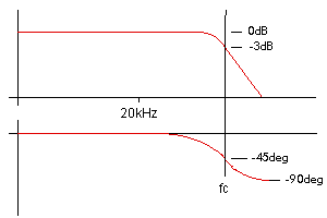
The differential input stage has mutual conductance gm. Assuming the second stage to have sufficient open-loop stage gain over the frequency range of interest, the amplifier open loop gain is given by gm/jwC. The closed loop gain is defined by the feedback resistors R1 and R2, and is fairly flat at low frequencies where the loop gain is high. The closed-loop gain and corresponding phase angle are shown in the next diagram:
The -3dB closed-loop frequency fc is proportional to gm/C.
Both gm and C may vary with signal voltage. Input stage gm variation is analysed in the 'Input Stage Distortion' article. For a single transistor second stage C includes the collector-base capacitance which has a highly non-linear voltage dependance. Any variation in gm or C resulting from an input signal will change the -3dB closed loop frequency, and so both amplitude and phase diagrams are moved backwards and forwards along the frequency axis. At any given frequency, particularly at high frequencies close to fc, the gain and phase shift will then vary with signal amplitude. A large low frequency signal will, for example, modulate both the phase and amplitude of a smaller high frequency signal, and so there will be both amplitude and phase intermodulation distortion.The solution to this problem is not difficult, just improve the input stage linearity with local feedback, and either use a cascode second stage or add an emitter follower in front of the second stage so that the non-linear capacitance feeds back into a low impedance and has little effect.
One 'solution' sometimes suggested, which will help very little if at all, is to add a resistor in parallel with the compensation capacitor C, and some other equivalent methods intended to increase the open-loop -3dB frequency. The addition of any resistor in parallel with C will increase the input stage differential input at all frequencies, and therefore increases the nonlinearity in this stage, while also reducing distortion reduction from overall negative feedback. Even ignoring this increase in input stage nonlinearity, I did an approximate calculation which showed that adding a resistor to increase open-loop -3dB frequency to 20kHz when using only 20dB feedback gave a reduction in phase modulation only by a factor of 1.1. As in the case of TID it is not the open-loop bandwidth we need to worry about, it is the feedback loop gain which we need to maximise at audio frequencies. If stability considerations permit this the reduction of C will be of benefit, and what this is doing is increasing the gain-bandwidth product, which is also what we need to increase to reduce TID.To avoid calculations we only need to observe that the frequency and phase responses above are the closed-loop responses, and the effect of variations in fc will be greater the closer we get to fc, and will reduce the further below fc we go. To keep the effect low at 20kHz we need fc to be far greater than 20kHz. This can be achieved, for example, with a mosfet output stage and heavy overall feedback, which can give 60dB or more feedback loop gain at 20kHz and virtually flat amplitude and phase at that frequency with very low sensitivity to small changes in gm or C. The open-loop gain can be allowed to increase almost indefinitely with reducing frequency. As with TID the low feedback, wide open-loop -3dB bandwidth approach appears to be unhelpful. Actually, even the closed-loop -3dB frequency is not entirely relevant, because if we add a capacitor across the overall feedback resistor the -3dB closed loop frequency can be reduced without increasing PIM.
Another approach is to take the high frequency compensation capacitor back to the input as in the following example:
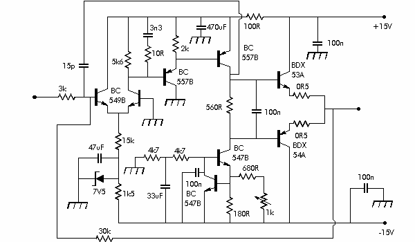
The following circuit is the class-B amplifier I used in 1977 for my distortion tests. The bridge-nulling technique was used to extract the distortion. Harmonic distortion at 2kHz was only 0.0006% at 7V rms output, but one reason it was so low is that a 22ohm resistive load was used. The purpose was to test the distortion extraction circuit, not the amplifier, which was just made as an example. It uses Darlington output transistors, and a two transistor driver stage.The 15pF high frequency compensation capacitor is connected to the input stage, an idea I adapted from an earlier design by John Linsley Hood (Hi Fi News Nov.1972-Feb.1973). I found an even earlier use of a similar method in '30 watt High Fidelity Amplifier' by Arthur R. Bailey, (Wireless World, May 1968), which takes a compensation capacitor to the input transistor emitter in a non-inverting design but has similar advantages. The article also mentions the problem of non-linear driver stage transistor capacitance, and the importance of selecting transistor type to minimise this. This high frequency compensation method helps to reduce slew rate and TID problems. The open loop gain is now primarily determined by a fixed passive resistor and capacitor, almost entirely avoiding the PIM mechanism described above. (In practice this may not be totally effective because it is sometimes necessary to add components such as the 3n3 plus 10R in the diagram above to stabilise the feedback loop.) Phase effects still exist in the amplifier tested, including those caused by the various non-linear transistor capacitances, as shown in the following test results.
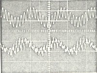
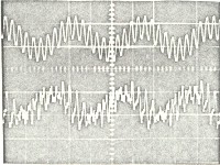
The test signal is a sum of 2kHz and 20kHz sine waves, each 5V peak amplitude, shown in the top traces. The distortion is shown in the lower traces, and clearly there is some breakthrough of undistorted signal here. What can still be clearly seen is that the 20kHz signal is cancelled well only over part of the 2kHz wave in the first diagram. Adjusting amplitude compensation in the bridge circuit could make no improvement to the uncancelled signal, but adjusting the phase gave the second diagram, where the cancellation is improved over one part of the 2kHz wave but worsens over the part where it was originally good. This shows that the phase of the 20kHz signal is being modulated by the 2kHz signal. The relative amplification of the lower traces compared to the upper traces is around 80dB, and the calculated peak to peak amplitude of phase modulation is about 0.006 degrees. That such a low level can be detected shows that this is a very sensitive test method. For comparison, a 5kHz signal from a speaker drive unit in the presence of a lower frequency causing just a 1mm cone excursion will have phase modulated by 6 degrees, i.e. a thousand times higher than the effect of this simple amplifier.
To summarise, both TID and phase intermodulation in the audio frequency range can be reduced by an increase in gain-bandwidth product, but in addition to this local feedback to linearise the input stage and steps to reduce the effects of non-linear capacitances can be helpful.
There is an alternative way to avoid the 'single frequency PIM' mentioned earlier, which is to use a square-law device as the input stage, e.g. a single undegenerated fet. For a sine wave applied to a square-law device there is a second harmonic and a dc term in its output, both of which are proportional to signal amplitude squared, but the fundamental term has the same gain at all signal levels. With the more common differential stage using either fets or bjts, there will be a cubic term, (and other higher order terms), and then there is an additional output term at the fundamental frequency proportional to input amplitude cubed. The gain of the stage therefore varies with signal amplitude as shown here. The square-law device unfortunately only avoids (or reduces) the phase shift effect for a single sine-wave, but with two frequencies there will still be phase intermodulation. To reduce both effects an input stage having only small variation of gm with changing output current level is needed, and this was compared for different input stages on my 'Input Stage Distortion' page. The best of those compared was the bjt complementary feedback pair, which has primarily second harmonic distortion, which as suggested may also be some advantage.
PIM Calculation
To confirm that for the reduction of PIM there is no advantage in adding a resistor in parallel with the compensation capacitor to increase open-loop bandwidth I did a simplified calculation. I was only checking the effect of adding the resistor, and there are some nonlinear effects excluded by this simplification, so it is not 100% accurate.
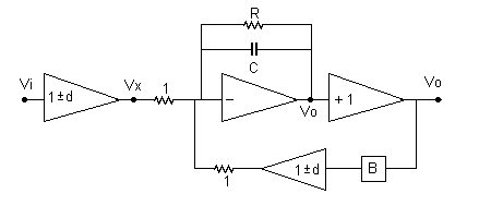
Here is the circuit I started from, showing the simplification. The input stage is split into two separate stages so that the phase modulation can more easily be separated from the amplitude modulation. Vx is an amplitude modulated version of Vi, but this effect is what we want to ignore, and the phase difference between Vo and Vx turns out to be more useful because the modulation is then confined to the real part of the transfer function. The input stage is represented by a unity gain stage with a resistor from its output to the inverting driver stage, which is assumed to have sufficient open-loop gain so that its closed-loop gain is determined entirely by R and C. A large low frequency signal modulates the gain of the input stage so that its gain varies from 1-d to 1+d, where d is assumed to be small. A low level 20kHz signal then has its phase modulated by this gain variation.
Adding currents at the input of the driver stage,
Vx + BVo (1 +/-d) + Vo/R + Vo.jwC = 0
Therefore ... Vo ( B +/-Bd + 1/R + jwC ) = -VxThe magnitude of the closed-loop phase shift is the phase angle of the expression in brackets. If the jwC part is assumed to be constant for now, then the effect of d on the real part is what we are interested in. Putting in some figures, suppose B = 0.05, to give a closed-loop amplifier gain of 20, and R = 200 gives 20dB negative feedback loop gain. If R has been chosen to give a 20kHz open-loop frequency response then wC = 1/200 = 0.005.
The real part now becomes ( 0.055 +/-0.05d ), a variation of +/- 0.9% if d = 0.01
With R omitted it becomes ( 0.050 +/-0.05d ), a variation of +/- 1% if d = 0.01
Assuming d is small, the change in phase has been reduced by about 10% by including R, so it does have some benefit. If the phase modulation was 0.11 deg without R it would be reduced to 0.10 deg with R.
Unfortunately the value of d is also affected by R, and to take an extreme example, with the low frequency component at 20Hz removing R will reduce the input stage signal by 1,000 times, and with distortion proportional to signal amplitude squared for a typical differential input stage d will fall by a factor of 1,000,000. Adding R therefore has two effects, one reduces phase modulation by a factor of 1.1, the other increases it by a factor of 1,000,000. Evidently R is a bad idea and should be omitted. The difference between the two effects may not be so extreme using different signal frequencies or different component values, and the calculation is not exact, but even so there seems little possibility of R reducing phase intermodulation effects.A similar conclusion was reached in my article about TID, where including R raised the steady state error voltage above the transient error voltage and increased both transient and steady state distortion in the input stage.
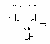
Input Stage Gain Variation
Assuming two identical transistors, having equal collector currents with zero input voltage,
with input Vi the differential output current, (I1 - I2), is proportional to tanh(Vi/2Vt)
where Vt =26mV at 25 deg.C.
Expanding the tanh function as a power series:
tanh x = x - x3/3 + 2x5/15 - 17x7/315 + ...... an infinite series. (for |x| less than pi/2)
If the current source It in the diagram is 1mA, then the first two terms of the power series are:
(I1 - I2) = Vi/52 - Vi3/421824 where Vi is in millivolts.Suppose Vi = A sin(wt) where A is in millivolts.
Using the formula sin3(x) = 3sin(x)/4 - sin(3x)/4
(I1 -I2) = A sin(wt)/52 - A3[(3sin(wt)/4 - sin(3wt)/4] / 421824.As an example, with 2mV peak input signal the 3rd harmonic component will be 0.025% of the fundamental level.
The fundamental terms are all we need to work out the stage gain, and then
(I1 - I2) = Asin(wt)[1/52 - 3A2/1687296]
The gain is then proportional to (I1 - I2)/Vi which is
1/52 - 3A2/1687296Substituting various values for signal amplitude A we find:
At 1mV input, the gain falls by 0.009%
At 5mV input, the gain falls by 0.22%
At 20mV input, the gain falls by 3.6%
These figures become increasingly inaccurate at higher voltages because we have only used the first two terms of the power series, and the higher order terms can be expected to become increasingly important as signal level increases.