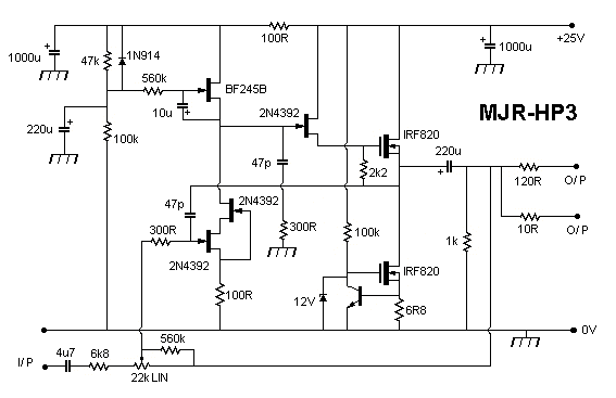
Headphone Amplifier Design.
To make a new design worthwhile I wanted to try something fairly unusual, and the starting point was to use an active volume control circuit. The best source of ideas I have seen is a Wireless World article by Peter Baxandall. ('Audio gain controls' Part 1, Oct.1980 p57-62, Part 2, Nov 1980 p79-83), which included one example dating back to 1939. The simplest active control from that article is of the type shown next:
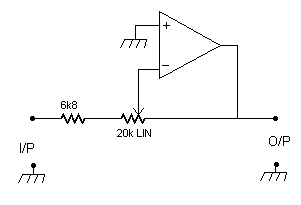
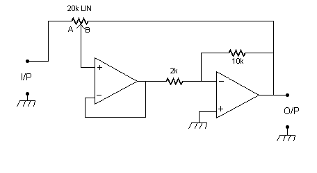
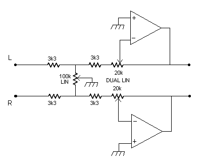
With these component values, with the wiper at the right end of the track the gain is zero, and at the left end it is about 9.3dB. This type of volume control has one big advantage, which is that a reasonable approximation to a log control law can be achieved with a linear pot. The result is only accurate over a limited range of gain, but conventional 'log' potentiometers are often far less accurate. Dual linear controls are generally found to be more accurately matched than the log versions, but there may be some variation in total track resistance for the two channels, and in the circuit above this will affect channel balance. The next circuit was suggested by Baxandall to avoid total track resistance having an effect, now only the ratio of the two sectors A and B of each track determine the gain, and this was found to be reasonably well matched in typical dual controls.
What is missing from both examples of this circuit is a balance control. This may not really be essential for use with digital signal sources where channel balance will usually be adequate, but some of us still use compact cassette players and other outdated signal sources, and here there may be a need for adjustment. There are a few ways to add a balance control, and one is shown next:
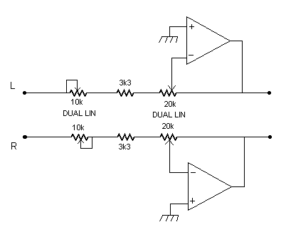
This just adds a dual linear pot in series with each input, connected so that adjustment increases one while decreasing the other. A single adjustment will compensate for different track resistances in the volume control, but unfortunalely any compensation for signal source channel imbalance will need to be readjusted whenever the volume is changed. What we want is for a single balance setting to remain correct at all volume settings, and although not perfect in this respect the next variation may be better.
Here only a single 100k linear control is used, and near the centre of the range there will be little effect, so very fine adjustment is easy. At extremes of the balance range there is a significant reduction of the input impedance on one channel.
I have one more variation shown next, which is my current favourite.
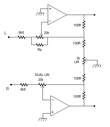
This is based on Baxandall's Fig.11, part 1, p59. He included this as a way to increase the gain, not as a way to add a balance control, but with a 2k linear control added this allows the balance to be adjusted in such a way that it is affected very little by volume setting. Unfortunately we are still left with the effect of differing track resistances for the dual control. We could just accept this as a small inconvenience, but the effect can be cancelled by adding just one fixed resistor in parallel with whichever track has the higher resistance, and is shown as Rp in the diagram. The value is easily calculated after measuring the track resistances with a multimeter.
If the higher value track measures R1 and the lower value is R2, then the value of Rp needed in parallel with R1 is:
Rp = ( R1 x R2 ) / (R1 - R2)One big advantage of this circuit compared to the two previous examples is that the input impedances of the two channels will be almost identical, and affected very little by balance adjustment. A small disadvantage is that the minimum volume setting does not give zero output, but with the small 100R resistor from the output the attenuation should be adequate for most applications. Potentiometers generally have some small track resistance at minimum setting, so zero output will not be achieved anyway.
To ensure output falls to a low level if the volume control wiper momentarily loses contact a resistor around 200k can be added from output to wiper, and 1k resistors from the ends of the balance control to earth will prevent the earth path being lost if the balance wiper loses contact.
The MJR-HP2.
In all the variations above the control wiper supplies the input current to an amplifier, and to prevent noise when adjusting the volume we need to keep this current low, and so a jfet input is a good idea. A mosfet input would be even better, but mosfets generally have poorer noise, so to keep current low a jfet can be used at a low drain voltage, and this can be achieved by using a cascode stage.
Headphones can be damaged by excessive dc, so some form of protection is needed to protect against fault conditions, and the use of capacitor coupling is the simplest idea, but as with my mosfet power amplifiers this can be included inside the overall feedback loop to reduce any distortion and keep the output impedance low.The HP2 uses just four fets. The BF245B current source is slightly unusual, but is an old idea, for example it is shown in a 1970 National Semiconductor application note AN-32 'FET circuit applications', on page 5. It has a high impedance at audio frequencies where the 10u capacitor keeps the gate-source voltage constant, but is a lower impedance at dc and so has the advantage of being able to set the dc operating level, and it can be used to keep the switch-on pulse slow and therefore low in amplitude. The output mosfet is shown as a 2SK213 low power lateral type, available from Dalbani for £3.50, but this is not really essential, and the circuit should work almost as well with a cheaper vertical type such as the IRF510. In either case a small heatsink is needed. A balance control similar to the earlier circuit could be included.
Initial testing reveals poor supply rejection and higher distortion than I would like at high frequencies or high output, so some further experimentation is in progress. One improvement is added supply filtering for the input stages, and this is included in the latest diagram.
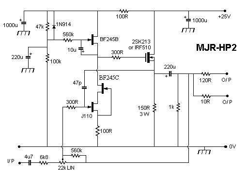
The increase in distortion at high frequencies is a result of driving the relatively high and nonlinear input capacitance of the mosfet output stage from a high impedance. The impedance can be reduced with an additional jfet buffer stage. The high frequency compensation is then no longer supplied by the mosfet capacitance, and so a compensation capacitor, shown here as 47p in series with 300R, must be added. There is some small indication of instability around 1MHz, so maybe the capacitance needs increasing, but there are other options I still want to try. Initial distortion tests show that at 100mV output the only detectable distortion is 2nd harmonic at 0.01% at both 1kHz and 10kHz. At 1V output there is 0.1% at both frequencies, with harmonics up to the 5th now visible, but falling with increasing order. An active current source is used in the output stage in this version, and different fets. These were donated by Richard Thomas, who also designed a board layout and built the first prototypes. The original fet types should work equally well.