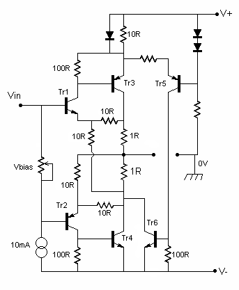
The first feedforward amplifier output stage described had limitations which were to a great extent avoided in a later version. Going back to the basic version shown next, there may be another way to overcome the problems. (To keep the diagrams simple two transistors are used in place of the original triples, and 10R feedback resistors in place of 100R).
The problem is that we require the top half to remain conducting in class-A at all times so that it can act as a feedforward error amplifier and cancel the effect of the lower half switching off over part of the signal cycle. The voltage drop across the 10R feedback resistors in the lower half when it drives a high current into the load will be sufficient to cause the top half to switch off unless the quiescent current is set very high. The 'circuit design' section describing this basic amplifier suggested an addition to sense the minimum current through the top half and adjust the current source (shown here as 10mA), but this was only intended as a slow quiescent current stabilising circuit. To prevent the error amplifier cutting off when the signal level changes suddenly a faster acting solution is needed, but if this is used to vary the 10mA current source then this will be a source of distortion, with a current pulse near the signal peaks.
There is an alternative way to add the correction signal such that any distortion will be cancelled by the feedforward stage, and this is shown next.
The current through the top half passes through a 10R resistor from the positive supply, while a diode in parallel limits the voltage drop at higher currents. When this current falls below for example 20mA, then Tr5 starts to conduct, and this turns on Tr6, which causes more current to flow in Tr3, preventing it from switching off. The signal injected by Tr6 is prevented from reaching the load by the error amplifier, Tr1 plus Tr3, inverting the signal and adding the original and inverted versions through the 1R resistors to give cancellation. This circuit has not been tried, so the component values should be regarded as suggestions rather than exact final values.
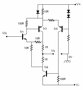
We now have two power transistors, Tr4 and Tr6, driving the negative current into the load, and the next idea is to eliminate one. It appears that we could remove both Tr4 and Tr2 as shown next, so that the entire negative output current is supplied by Tr6. Better still we can remove the 10mA current source and bias adjustment.
By adjusting one of the 10R resistors connected to Tr1 emitter the crossover distortion can be more accurately nulled. There may be some advantage in using a power mosfet for the lower transistor, Tr6, and examples are shown later. Even further simplification is possible. It may be that good results are still possible if the 'error amplifier' is just designed to have high local feedback and consequently low output impedance, so then the error signal current has little effect.
This is no longer a feedforward design, and is not my own idea, it was invented by P.L.Taylor, and his circuit, very similar to that above, was published in Wireless World, June 1973, pp 301-302. This used only 6 transistors for a complete power amplifier with 30W output and no bias adjustment required. Distortion was specified as 0.1% 'mainly second harmonic'. Using a triple in place of Tr1 and Tr3 should reduce distortion considerably, but then stability becomes a more serious concern, there already being 4 transistors in a feedback loop without this addition, so some form of stabilisation may be needed.
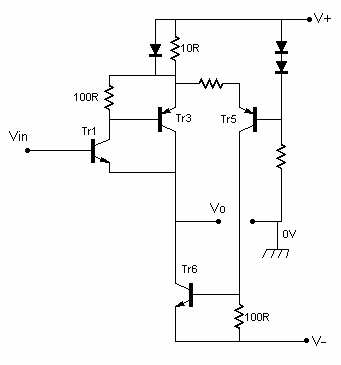
1.Nov.2006. Further thought suggests that the third circuit on this page could be developed a little firther. First, changing the lower transistor to a mosfet and using a triple for the error amplifier to make it a bit more realistic:
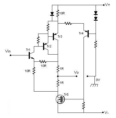
A problem with this is that the triple includes a relatively slow power device, which will limit the performance, and the output is then fed through a mosfet device, adding more phase shift and so reducing even more the level of feedback possible without instability. A great advantage of the Quad 'current dumping' circuit was that the error amplifier was a relatively low power class-A amplifier with heavy feedback and good linearity, with the slower power devices kept separate. To remove the power device from the error amplifier the next arrangement is a possibility:
Here the diode across the current sensing resistor is replaced by the base-emitter junction of the power device, Tr6. The triple is no longer required to provide all the positive output current, and lower power but faster devices can be used, which in principle at least makes higher feedback possible. As for the Quad amplifier, the quiescent current is now just the operating current of the low power error amplifier, and there is no bias adjustment or stabilisation needed. Tr6 remains switched off until output current above a certain level is needed, very much like Quad's current dumpers. The 1 ohm resistors can be reduced to any convenient value, they are part of the feedforward error cancellation, but no longer determine quiescent current value or thermal stability. One problem with the Quad circuit was that the non-linear input impedance of the current dumper stage directly loaded the output of the error amplifier, and this source of non-linearity was reduced by feedback, but not cancelled by feedforward, so it could not even in theory be reduced to zero. By sensing the error amplifier current at the supply rather than the output this non-linear loading is avoided. (Variations of the Quad circuit which avoid the problem have been published, but I don't know if Quad ever found it worthwhile adding these 'improvements'.)
My own circuit seems likely to have stability problems, and for this reason is unlikely to compare favourably to my MJR7 mosfet design.11.Nov.2006. Here is another variation, a complete amplifier using just an op-amp plus 4 transistors. The more I look at this the less I believe it will work well, and I don't entirely trust simulations, so I may have to actually build this one to convince myself. (It may need a few changes from the basic diagram, as is usually the case with my 'theoretical designs'.)
The OPA552 may not be the best choice of op-amp, but I just happen to have one. The op-amp input noise voltage is a little higher than I would like, but on the plus side the distortion is very low, about 0.0015% at 20kHz at 15V rms output with gain 5, it has 12MHz gain-bandwidth, and the maximum total supply is 60V. It is only stable for closed-loop gain 5 or more, so with a 10p across the feedback resistor it may be unstable, but 100p at the input prevents this, and is a good idea anyway to more accurately define feedback level at high frequencies, and to help reject interference above 1MHz. (This arrangement of capacitors is also shown in the data sheet for the OPA552, but for different reasons.) Using the op-amp in an inverting circuit, and with low output current taken only in one direction we can avoid both common-mode and crossover distortion, and the distortion figure achieved may be well below that specified. The PSRR falls at high frequencies so at least an RC filter on each op-amp supply is essential. Although no adjustment is needed it may be worthwhile adding a trimmer to more accurately null the power stage distortion. Maybe this could be adjusted without any test equipment just by touching the mosfet gate with a finger and adjusting the trimmer to cancel any resulting audible output to the speaker.
No overall feedback is taken directly from the output, one consequence being that the output impedance will be a little over 0.11 ohms, but still low enough to give an adequate damping factor for normal 8ohm speakers. Whether an output inductor is needed to achieve stability with capacitive loads remains to be seen.