Figure 7.1 Signal and Noise Pickup on Long Lines.
For a verbal description click here.
Chapter 7 Operational Amplifier Circuits.
7.1 Instrumentation Amplifier.
7.2 AC Voltmeter Circuit.
7.3 Open-loop Linearization.
7.4 Absolute Value Amplifier.
7.5 Log Converter.
7.6 Active Filters.
7.7 Problems.
7.8 Answers to Problems.
Chapter 7
Operational Amplifier Circuits.
The best thing about op amp circuits is that it is hard to keep them from working. Although none of the circuits in Chapter 6 was indicated as having been laboratory tested, you can build any of them and they will work! Because of this increased reliability over discrete transistors, anyone who works with electronic circuits prefers to use op amps whenever possible. Unfortunately today's low cost op amps will not perform much above the audio frequency band. If the frequency range permits, op amps are to be preferred over discrete transistors.Back to Fun with Transistors.
Back to Fun with Tubes.
Back to Table of Contents.
Back to top.
7.1 Instrumentation Amplifier.
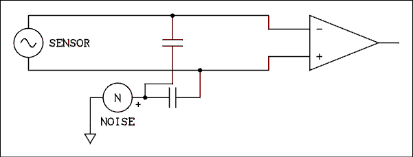
In laboratory instrumentation it is often necessary to place a sensor at some distance from the instrument to which it is connected. In such a case the long wires which connect the sensor to the instrument will act as antennas and pick up noise, (noise is any electrical signal which is in a place where it is not wanted). Using shielded cables will help but there may still be some noise pickup, especially if the voltage of the sensor is very small, requiring that the input amplifier of the instrument have a very high gain.
Figure 7.1 Signal and Noise Pickup on Long Lines.
For a verbal description click here.
The noise which is picked up on the wiring is usually common mode while the sensor is connected between the two wires so that its signal is normal mode. The situation is illustrated in Figure 7.1. Twisting the wires together to insure that they are in the same physical location will insure that the noise picked up on both wires will be the same. If the two wires are connected to the two inputs of a differential amplifier, the common mode noise on the wires will be cancelled out while the signal will be amplified. For this method of noise canceling to work properly the two inputs must have identical input impedances and gains which are equal in magnitude and opposite in sign. In addition to these requirements the gain is usually very high. An amplifier which meets all of these requirements is called an instrumentation amplifier and a circuit is shown in Figure 7.2.
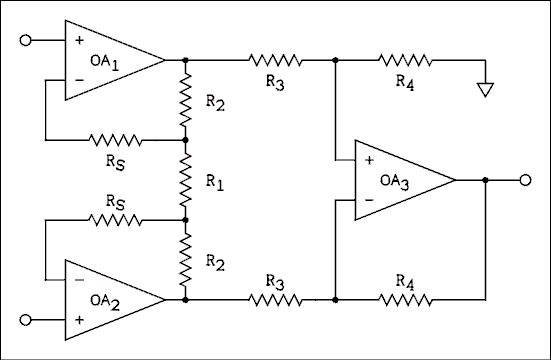
Figure 7.2 Instrumentation Amplifier.
For a verbal description click here.
The best way to approach a problem involving this circuit is to treat it as a circuit analysis problem. For example, we will calculate the gain of the first amplifier stage of the circuit of Figure 7.2. The first stage consists of OA1 and OA2. If a voltage is applied between the two inputs (normal mode) the two op amps will adjust their output voltages to bring each of the inverting inputs to the same potential as the corresponding noninverting input. If we apply a voltage of VIN between the two input terminals, the identical voltage will appear across R1. This will cause a current of,I = VIN / R1 (7.1) to flow in the series combination of the two identical resistors labeled R2 and R1. There is no significant drop across the two resistors labeled RS. The output voltage of the first stage is the total voltage drop across the resistor chain.VO = I (R1 + 2 R2). (7.2) Substituting equation 7.1 into equation 7.2 and dividing through by VIN gives,VO / VIN = (R1 + R2) / R1 (7.3) The gain of the second stage which consists of OA3 could be derived in the same way if desired. Rather than to have yet another equation to remember it is better to analyze the circuit using Ohm's and Kirchhoff's laws.Example 7.1.
In the circuit of Figure 7.2 R1 = 2 k ohms, R2 = 99 k ohms, R3 = 10 k ohms and R4 = 100 k ohms. If the voltage at the top input is +2.0 mV and the voltage at the bottom input is -1.0 mV, what is the output voltage?Solution:
The best way to keep track of voltages is to make a chart of all three terminals of all three op amps as shown. The voltages at the noninverting inputs of OA1
Terminal OA1 OA2 OA3 noninverting input +2 mV -1 mV 136.81818 mV inverting input +2 mV -1 mV 136.81818 mV Output 150.5 mV -149.5 mV 3.00 V and OA2 are given and so can be filled in immediately. The op amps will make the voltage at the inverting input be the same as that at the noninverting input and so these values can also be filled in by inspection. The voltage across R1 is 2 mV -(-1 mV) = 3 mV. The current in R1 is I = 3 mV / 2 k ohms = 3/2 uA. The voltage drop across either R2 is V = 3/2 uA x 99 k ohms = 148.5 mV with the upper end positive. The lower end of the top R2 is at a potential of +2 mV; therefore, the upper end of the top R2 is at 2 mV + 148.5 mV = 150.5 mV. The upper end of the bottom R2 is at -1 mV; therefore, the lower end is at (-1 mV) + (-148.5 mV) = -149.5 mV. Notice that the difference is 150.5 mV - (-149.5 mV) = 300 mV. This confirms a first-stage gain of 100. The voltage at the noninverting input of OA3 is found by simply applying the voltage divider equation to R3 and R4. The noninverting input of OA3 does not load the voltage divider. V+3 = VO1 R4 / (R3 + R4) = 150.5 mV x 100 k ohms / 110 k ohms = 136.81818 mV. The entries for both the noninverting input and the inverting input of OA3 can now be filled in. The voltage drop across the bottom R3 is 136.81818 mV - (-149.5 mV) = 286.31818 mV. The current through the lower R3 is I = 286.31818 mV / 10 k ohms = 28.631818 uA. The voltage drop across the lower R4 is 28.631818 uA x 100 k ohms = 2863.1818 mV with the right end positive. The voltage at the output of OA3 is its inverting input voltage + the drop across the lower R4, which is 136.81818 mV + 2863.1818 mV = 2999.99998 mV which, when rounded off, gives 3.00 volts.
The results of this example confirm that the gain of the second (OA3) stage is given by
A' = R4 / R3 (7.4) even though the circuit appears more complicated than an ordinary inverting amplifier.The input to the circuit of Figure 7.2 is a differential input because neither side of the input needs to be connected to ground. The output of the first stage (OA1 and OA2) is a differential output because neither side is connected to ground. The input to the second (OA3) stage is also differential. The output from OA3 is said to be single-ended because one side is connected to ground. Thus a circuit consisting of two R3s, two R4s and an op amp can be used to convert a differential source to a single-ended load. The problem with using such a circuit is that the input resistances at its two inputs are not equal. The input resistance at the noninverting input is R3 + R4 while the input impedance at the inverting input is R3. The two noninverting amplifiers serve to balance the input impedances and at the same time make them very high.
Connecting R1 between the two amplifiers instead of each amplifier having its own R1 makes the amplifiers self-balancing, which increases the common mode rejection ratio. Note in the example that even though the original inputs had a 2 to 1 imbalance, the outputs had less than a 1% imbalance. The OA3 stage can easily accommodate the small imbalance. If this circuit is to have a high CMRR the values of the two R3s and the two R4s must be very well matched.
The resistors RS are used to prevent serious imbalance due to input bias currents in the event that the source has a high Thevenin resistance. If input bias current is no problem the two resistors may be omitted (replaced by pieces of wire).
Back to Fun with Transistors.
Back to Fun with Tubes.
Back to Table of Contents.
Back to top.
7.2 AC Voltmeter Circuit.
Voltmeters, whether analog or digital, are basically DC measuring instruments. When it is desired to measure AC the common practice is to change the AC to DC and then measure it. This causes problems because the diodes which are used to rectify the AC are not linear. Perhaps the oldest approach is to print a separate scale on the face of the meter, (analog meters), and instruct the operator to read that scale when measuring AC. This method has worked well for many decades in meters which have no electronic circuits inside them.Electronic voltmeters use some electronic tricks to make the response of the rectifiers linear. The circuit of a linear AC voltmeter is shown in Figure 7.3.
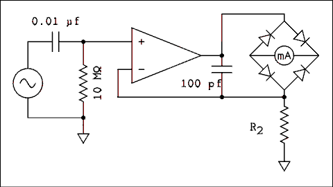
Figure 7.3 Linear AC Voltmeter Circuit.
For a verbal description click here.
If you trace the current through the bridge as was done in Chapter 3 the current will be seen to be flowing in or out of the op amp output, through one of the top diodes in the bridge, through the meter from right to left, through one of the bottom diodes and up or down through the resistor R2 to ground. The feedback is taken from the top of the resistor which makes the voltage waveform across R2 match the input waveform. Because R2 is a resistor, its current waveform will match the input voltage waveform. The meter and the resistor are in series. The same current is flowing in the meter as flows in R2. The meter current is the absolute value of the R2 waveform but the magnitudes are identical. If you look at the output voltage waveform on a scope, you will see a very distorted wave. What you are seeing is what has been said many times, "The op amp will adjust its output voltage to make the inverting input voltage equal the noninverting input voltage." The output voltage will be whatever it has to be to make the current in R2 directly proportional to the input voltage. In this case it is the meter current which is being linearized. Since the pointer responds to the meter current, the deflection of the pointer will be linearly proportional to the average input voltage. The meter can be calibrated to indicate the RMS of a sine wave.The value of R2 sets the full-scale range of the meter. With the value given the range will be approximately 1 volt if a 1 mA meter is used. The 100 pf capacitor is to prevent the op amp from oscillation at high frequencies. This capacitor will cause the meter to lose accuracy at high frequencies and if you want to measure voltages of high frequency waves the capacitor must be as small as possible while still preventing oscillation. The capacitor at the input is necessary to block any DC which may be mixed with the AC to be measured.
Back to Fun with Transistors.
Back to Fun with Tubes.
Back to Table of Contents.
Back to top.
7.3 Open-loop Linearization.
Occasionally in a physics lab it is necessary to make a measurement on some sensor which is at a very high potential. When this is the case a way must be found to transfer the electrical signal and still not have any direct electrical connection. That may seem impossible but don't forget about the transformer which transfers electrical energy while providing electrical isolation. If the sensor delivered AC, a transformer could be used to couple the signal while isolating it. Unfortunately most sensors deliver a slowly changing DC. One approach often used is to change the DC to a proportional AC and then pass it through a transformer for isolation. After isolation the signal may be processed in any manner desired.
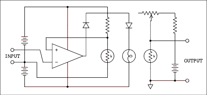
Figure 7.4 Open-loop Linearized Photocell.
For a verbal description click here.
A somewhat simpler method of isolation is shown in Figure 7.4. The input signal (from the sensor) is applied to the inverting input of the op amp. The feedback is taken to the noninverting input of the amp. That may seem to be positive feedback but the lamp and photocell have something to say about that. As the voltage at the output of the op amp goes positive, the lamp grows brighter. As the photocell receives more intense illumination its resistance decreases. As the resistance of the photocell decreases the voltage at the noninverting input of the op amp will be decreased. The combination of the lamp and photocell provide the inversion and so the op amp does not have to.When a positive voltage is applied to the input the op amp will adjust the brightness of the lamp so that the voltage across the photocell on the left is equal to the input voltage. If the two photocells are closely matched the voltage across the photocell on the right will also be equal to the input voltage. Because there is no electrical connection between the two parts of the circuit, the input can be at any arbitrarily high potential and allow the output to be grounded.
In this circuit the batteries are meant to be batteries. The circuit should be constructed in an insulated box to prevent accidental electric shock. The value of the resistor and pot which are in series with the photocells depend on the illuminated resistance of the photocells. The values of these resistors will have to be determined after the photocells are obtained. The purpose of the two diodes in series with the lamp is to permit the lamp voltage to go all the way to zero. The output of an op amp will have a minimum voltage of 2 P-N junctions from the negative power supply lead. The circuit only works for positive input voltages. If a negative input is applied, the lamp will attempt to get darker than dark and nothing will happen, except in the twilight zone.
Back to Fun with Transistors.
Back to Fun with Tubes.
Back to Table of Contents.
Back to top.
7.4 Absolute Value Amplifier.
The AC voltmeter circuit given above will change AC to a linear meter reading but sometimes it is necessary to change an AC to a linearly proportional DC voltage. Simple rectifiers of the type used in power supplies are not linear and indeed have no output for the first 0.6 volts of the input signal. If the diodes are placed in the feedback loop of an op amp (two op amps in this case) the rectified output will be directly proportional to the input. The circuit of a linear rectifier or absolute value amplifier is shown in Figure 7.5.
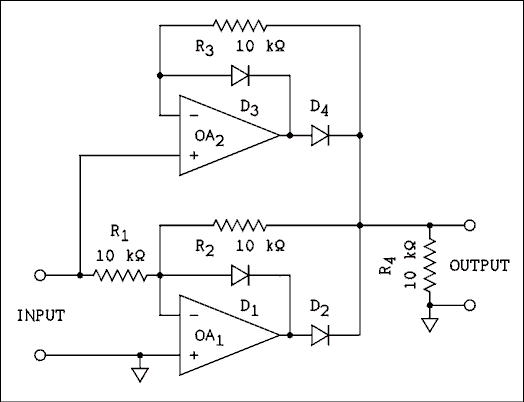
Figure 7.5 Absolute Value Amplifier.
For a verbal description click here.
When an AC signal applied to the input goes positive, the output of OA1 goes negative. This reverse biases D2 and forward biases D1. The output of OA1 is disconnected from the output of the circuit. Meanwhile, the output of OA2 goes positive. This forward biases D4 which connects the output of OA2 to the output of the circuit. D3 is reverse biased as we will shortly see. The inverting input of OA2 is connected to the output node through R3. The op amp will adjust its output to whatever voltage is necessary to bring the output node to the same potential as the input node. That will cause the output of OA2 to be about 0.6 volts more positive than the input node of the circuit. D3 is therefore reverse biased by 0.6 volts. For a positive input, the output is also positive and has the same voltage.When the input goes negative the output of OA2 goes negative, which reverse biases D4, disconnecting the output of OA2 from the output node of the circuit. D3 is forward biased. For a negative input, the output of OA1 will go positive. D2 is forward biased and D1 is reverse biased. Resistor R2 takes feedback from the output node and if R1 and R2 are of equal value the output node will have the same magnitude and opposite sign as the input node. Thus for a negative input the output is positive but has the same magnitude as the input.
If a capacitor is placed in parallel with R4 the circuit becomes a peak detector. If an RC low-pass filter is connected to the output the circuit becomes an average value detector. In the latter case the resistor in the low-pass filter should be greater than 1 M ohms for an error of less than 1%. In either case the value of the capacitor will depend on the response time required.
Back to Fun with Transistors.
Back to Fun with Tubes.
Back to Table of Contents.
Back to top.
7.5 Log Converter.
This section has been rendered obsolete by the low cost of powerful desk top computers and data collection systems. It has been left in to show how things were a few years ago.If it is necessary to take the log of data which is being collected in an experiment, the method of choice is to digitize the data and let a computer do the log taking. In very well-funded laboratories the computer is on-line, (connected to the experimental equipment). In less well-funded experiments the data must be hand carried - on disk, tape or paper - to the computer.
It is always desirable and often necessary to see the log of the data as the experiment is running. Seeing the log of the data may be necessary in order to properly adjust the equipment. If the experimenter is able to see the data come out as the experiment runs, it is possible to tell if something has gone wrong. A strip-chart recorder is often used for this purpose.
Many experiments deliver the data in analog form and most strip-chart recorders accept data in analog form. For the purpose of so-called "quick look" data reduction an analog device which will take the log of analog data may be helpful.
The circuit of a working logarithmic converter is shown in Figure 7.6. This circuit is designed to be used with a strip-chart recorder having a Y axis input of 10 mV full- scale. With the values given the unit may be calibrated to 1 mV = 10 dB. The converter operates from two 9 volt transistor radio batteries.
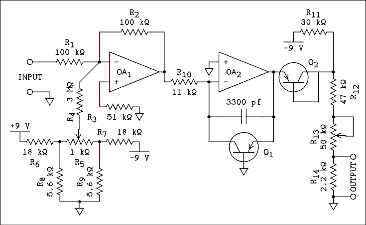
Figure 7.6 Logarithmic Converter for Use with
a 10 mV Strip-chart Recorder.
For a verbal description click here.
The op amp is a type 558 which has two amplifiers in a single 8 pin package. The transistors used here were from the junk box. Any low power PNP transistors will do so long as they are reasonably well matched.The batteries are connected as shown in Figure 6.1. A double pole switch is required to interrupt the current from both batteries.
The input signal is applied through R1 to the inverting input of OA1 which is nothing more than a unity-gain inverter. R5 is a zero adjust control. The op amp used has no offset adjustment pin connections and so the somewhat elaborate network of R4 through R9 is required to provide offset adjustment for the op amp.
Transistor Q1 is the element which does the log taking. The I-V curve of a P-N junction is an exponential or a logarithmic function depending on how you look at it. In this circuit we are looking at it as a log function. If a positive input signal is applied to the input, it will be inverted and appear at the output of OA1 as a negative voltage. This will cause current to flow to the left in R10. The output of OA2 will adjust itself so that the collector current of Q1 is equal to the current in R10. The voltage at the op amp's output will be adjusted so as to forward bias the base-emitter junction of Q1. If the input voltage changes, the collector current of Q1 will change linearly and the base-emitter voltage will change logarithmically.
Transistor Q2 serves to temperature compensate the circuit. For example, if the temperature goes up, the base- emitter voltage of Q1 will decrease, which will lower the output voltage. At the same time the temperature of Q2 will increase and its base-emitter voltage will also decrease. The decreased drop across Q2 will increase the output voltage which will compensate for the decrease caused by Q1. Q1 and Q2 should be in physical contact to insure that they are at the same temperature. If the transistors are in metal packages, they should be electrically insulated from each other because the case is often connected electrically to one of the transistor elements.
The network of R12 through R14 reduces the output voltage to the proper level for the 10 mV chart recorder. R13 should be adjusted for a span of 10 dB per mV at the upper end of the working range. R5 may be used to correct errors at the low end of the range. The unit will not have a working range of 100 dB as implied by 10 / mV over a range of 10 mV. The best achievable is about 50 dB. Below -50 dB the response tends to become linear rather than logarithmic.
If the input voltage is negative, OA2 will go to full negative saturation which will slam the chart recorder's pen down hard against the zero stop. The log of a negative number is undefined in the analog world as well as in the world of numbers. The only capacitor in the circuit is to prevent OA2 from oscillating at ultrasonic frequencies.
Back to Fun with Transistors.
Back to Fun with Tubes.
Back to Table of Contents.
Back to top.
7.6 Active Filters.
A single RC filter provides a roll off in the stop-band of 20 dB per decade. Cascading filters (connecting the output of one to the input of the next) does not work as well as might be expected. The roll off around cutoff is so gradual that the filter begins to affect the output long before any large values of attenuation are reached. A single LC filter section will give a roll off of 40 dB per decade and it affects the output only slightly on the pass-side of cutoff. Attenuation increases quickly on the stop-side of cutoff. The problem is that inductors are large, heavy, expensive and often difficult to find. The solution is an active filter. An op amp circuit which has only resistors and capacitors in addition to the op amp can simulate an LC filter. Several of such circuits could be placed in the same volume of one inductor.Figure 7.7 shows a high-pass filter circuit. In this circuit if C = 0.01 uf and R = 10 k ohms the cutoff frequency is 2.8 kHz and the attenuation at 60 Hz is 50 dB. The cutoff frequency can be calculated from,
fC = 1 / (3.5 R C) (7.5)
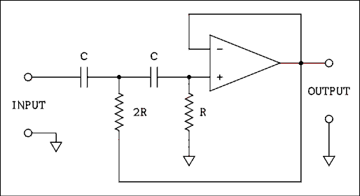
Figure 7.7 High-pass Active Filter Circuit.
For a verbal description click here.
The op amp is used as a unity-gain buffer. In order to insure good performance, the gain error should be less than the desired measurement accuracy at the highest frequency to be passed.Figure 7.8 shows a low-pass filter circuit. In this circuit if C = 0.1 uf and R = 150 k ohms the cutoff frequency is 4.5 Hz and the attenuation at 60 Hz is 36 dB. The cutoff frequency can be calculated from,
fC = 1 / (15 R C) (7.5)
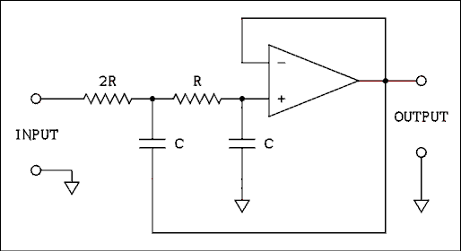
Figure 7.8 Low-pass Active Filter Circuit.
For a verbal description click here.
The op amp is used as a unity-gain buffer. In order to insure good performance, the gain error should be less than about 5% at 10 times the cutoff frequency.Example 7.2.
It is desired to construct a low-pass filter with a cutoff frequency of 0.1 Hz. The capacitors to be used have a value of 1.0 uf. (a) What is the calculated value of R? (b) What standard values should be used for the two resistors in the filter?Solution:
(a) Solving equation 7.6 for R gives R = 1 / (15 fC C) =
1 / (15 x 0.1 x 1 x 10-6) = 667 k ohms
(b) The closest value for R is 680 k ohms and the closest value for 2R is 1.3 M ohms.
Back to Fun with Transistors.
Back to Fun with Tubes.
Back to Table of Contents.
Back to top.
7.7 Problems.
- In the circuit of Figure 7.2 R1 = 200 ohms, R2 = 99.9 k ohms, R3 = 10 k ohms and R4 = 1 M ohm. If the voltage at the top input is -20 uV and the voltage at the bottom input is -70 uV, (a) what are the voltages at each of the op amp terminals? Make a chart similar to that in Example 7.1. (b> What is the gain of the amplifier?
- Using the circuits given in this chapter draw the schematic diagram of a circuit which will take an AC signal and rectify it without introducing significant errors. Then the circuit must average the rectified AC and convert it to dB.
- Design a high-pass filter which has a cutoff frequency of 10 kHz. The capacitors have a value of 0.0033 uf. Give the standard values for the resistors to be used in the circuit. Draw the circuit.
Back to Fun with Transistors.
Back to Fun with Tubes.
Back to Table of Contents.
Back to top.
7.8 Answers to Problems.
- The table shows the values.
Terminal OA1 OA2 OA3 noninverting input -20 uV -70 uV 24.7079208 mV inverting input -20 uV -70 uV 24.7079208 mV Output 24.9550000 mV -25.0450000 mV 5.0000000 V (b) 100,000
- The averaging could be accomplished using a passive RC filter but I decided to go all out. If you drew an RC filter, your answer is correct.
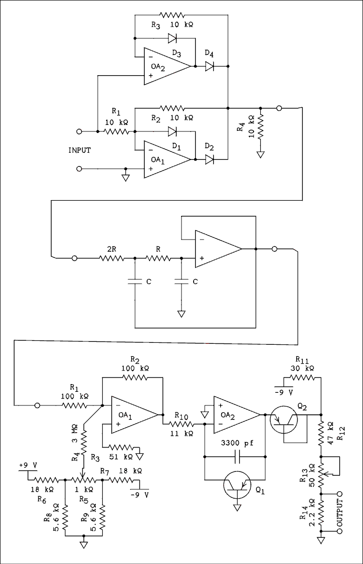
Figure 7.9 Answer to question 2.
For a verbal description click here.
- R = 9.1 k ohms, 2R = 18 k ohms. The circuit is like figure 7.7.
Back to Fun with Transistors.
Back to Fun with Tubes.
Back to Table of Contents.
Back to top.