For a verbal description click here.
I have received emails from some people who want to go on batteries. Others want to build signal processors into guitars. When you are limited in power and space, tubes are not the solution. Here are some circuits I have designed over the years and found to work well. If this page proves to be popular I will add more circuits to it.Impedance Buffer and Gain Block.
An impedance buffer is a device that allows a high impedance source to drive a low impedance load. For an example if you should want to use a ceramic phono cartridge to drive a small power transistor to in turn drive a small speaker it might seem to work by the voltage levels involved. The catch is that a ceramic cartridge has a high output impedance while the transistor has a low impedance. The cartridge just can't supply enough current to drive the base of that transistor.For the example given above a simple FET source follower or BJT (bipolar junction transistor) emitter follower would do the job. But in a more demanding application the problems with these types of buffers might not be tolerated. A FET source follower introduces considerable distortion and an emitter follower doesn't really isolate the load from the source. The input impedance is the load impedance times the transistor current gain. If the load changes the input impedance changes and that is not how an impedance buffer is supposed to work. And if the transistor develops a base to emitter short, a common failure mode, The circuit will test OK using an audio oscillator but all impedance buffering has disappeared and there is effectively a wire connected from input to output. This is one of the hardest problems in transistor circuitry to trouble shoot.
Then there is the problem of gain. FET source followers commonly have gains of 0.5 to 0.7. The gain is not very predictable which is another knock against it. The emitter follower has a gain of about 0.9 but changes in the load impedance are reflected in the load it presents. If you should want impedance buffering and a gain greater than unity your simply out of luck when it comes to source and emitter followers.
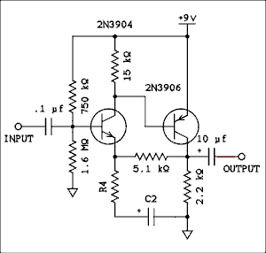
The Two Transistor Circuit.
The circuit below can be set to unity gain and used as an impedance buffer or set to a gain of greater than one and used as a gain block and buffer. At unity gain the input impedance is essentially resistive and has a value of 500 k ohms. As gain is increased the impedance is a little less but it still remains in the hundreds of k ohms.
For a verbal description click here.
The table below gives gain and distortion figures and the values of R4 and C2 required. Where the value is replaced by "--" The components should be left out.I taught an electronics lab for 33 years. When we did the experiment on op amps the instructions said to leave out a resistor to make a unity gain amplifier. About 1 in 10 students would substitute a wire for the resistor. I finally had to say "Leave out the resistor. Don't replace it with a wire. Leave the space blank. No resistor, no wire, no nothing." Got it?When I connect my low distortion oscillator into my analyzer it reads 0.015%. So all that can be said about the distortion at a gain of 10 dB or less is that the distortion is less than 0.015%. Component Values, Gains, and Distortion.
Gain dB R4 (ohms) C2 (uf) Distortion (%) 1.0 0 -- -- 0.015 2.0 6 5.1 k 10 0.015 3.16 10 2.4 k 22 0.015 10 20 510 47 0.050 31.6 30 160 220 0.17 Frequency response at 30 dB gain - 3 dB 7.6 c to 814 kc.
Open loop gain is approximately 280.
How It Works.
I've already made that joke. The following discussion is for the DC bias levels of the circuit. The voltage divider consisting of the 750 k ohm and 1.6 meg ohm resistors would hold the base voltage of Q1 at 6.1 volts if not loaded. The collector current of the 2N3904, Q1, flows through the 15 k ohm resistor and base of the 2N3906, Q2. The circuit is designed so the voltage at the collector of Q2 is 4.5 volts. When the voltage is 4.5 volts the collector current is 2.05 mA. The current gain of each transistor is approximately 100 so the base current of Q2 is approximately 20 uA (micro amps). The voltage from base to emitter of Q2 is 0.6 volts so the current in the 15 k ohm resistor is 40 uA. The collector current of Q1 is the sum of the resistor current and the base current of Q2. That is 60 uA. Then the base current of Q1 is approximately 0.6 uA. Allowing for the current gain to be a little low because of it's small collector current let's say the base current is 1 uA. Now when the output voltage of the 750 k ohm and 1.6 meg ohm is recalculated with that load it comes out to 5.5 volts. Now the voltage drop from base to emitter of Q1 is 0.6 volts and the drop across the 5.1 k ohm resistor is 60 uA x 5100 ohms = 0.3 volts. That makes the voltage at the collector of Q2 4.6 volts.If the voltage at the collector of Q2 is higher than it should be the emitter current of Q1 will be low because of the decreased drop across the 5.1 k ohm resistor. That leads directly to a decreased base current of Q2 and decreases its collector current. That reduces the drop across the 2.2 k ohm resistor decreasing the voltage at the collector of Q2. If the voltage gets low it will result in more current in Q1 and more collector current in Q2 which will pull the low voltage back up to where it belongs. The fact is that the voltage never wanders off to need correcting. It is constantly being corrected.
When an AC signal is applied to the base of Q1 the regulating effect causes the voltage at the collector of Q2 to follow along duplicating the exact wave form at the input. But the circuit has a high input impedance and a low output impedance.
When set to unity gain it has 100% feedback. When a series resistor and capacitor are connected from the emitter of Q1 to ground the percentage of feedback is reduced and the gain goes up. The input impedance is lowered slightly but remains quite high. The open loop gain of approximately 280, your mileage may vary, Limits the maximum gain to 30 dB.
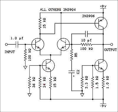
Five Transistor Circuit.
This circuit is obviously more complex than the other one but it offers better performance. It will deliver more output voltage at higher gains and lower distortion. It has been designed to operate from plus and minus 9 volts but probably could be used on plus and minus 12 without changes. If you want to run it from plus and minus 20 volts you should redesign it for that higher voltage. Its DC output voltage is very small so there is no need for a blocking capacitor.
For a verbal description click here.
Component Values, Gains, and Distortion.
| Gain | dB | R5 (ohms) | C2 (uf) | Distortion (%) | Distortion (%) |
| at 2 VRMS | at 3.5 VRMS | ||||
| 1.0 | 0 | -- | -- | n0.025 | 0.030 |
| 2.0 | 6 | 100 k | 1.0 | 0.020 | 0.020 |
| 3.16 | 10 | 47 k | 1.0 | 0.015 | 0.020 |
| 10 | 20 | 11 k | 4.7 | 0.020 | 0.020 |
| 31.6 | 30 | 3.3 k | 10 | 0.030 | 0.040 |
| 100 | 40 | 910 | 47 | 0.065 | 0.10 |
Frequency response at 30 dB gain, - 3 dB, 6 c to 133 kc
Open loop gain approximately, 1000
This circuit has several features in common with an op amp and is sometimes called a discrete op amp. The two NPN transistors which are side by side on the left are a differential pair and the one below them is a current sink. The current sink is set to 200 micro amps so if all were perfect the current in each transistor would be 100 uA. Even if there is a current unbalance the voltages at the two bases are very close to being equal. The left hand base is held to ground by a 100 k ohm resistor. The output terminal is connected to the right hand base by a 100 k ohm resistor. The output terminal will be regulated to be very close to ground or zero potential. The 10 pf capacitor is to prevent oscillation at ultrasonic frequencies.With R5 and C2 removed the gain is unity. When R5 and C2 are present the amount of feedback is reduced increasing the gain. The capacitor causes the DC level to be unchanged by the amount of feedback. The base current of approximately 1 microamp flows toward the transistor. That makes the base end of the resistor more negative than the other end. That's why the negative end of the capacitors goes to the bases.
I built the circuit twice with randomly selected transistors and it performed the same both times. So you don't need to worry about matching transistors. If you are determined to use a matched pair you should set up to measure the current gain at Ic = 100 uA. An alternative would be to use one of those ICs known as a transistor array. All transistors on a chip are matched.
Electronic Volume and Tone Controls.
Below are three circuits; a volume control, and two tone controls, one for bass and the other for treble. They all are controlled by a DC voltage instead of passing the audio signal through a pot. They all have in common the use of a device known as a Doubly Balanced Mixer. This device is often known as a Doubly Balanced Modulator. Which ever you prefer to call it, it can be abbreviated DBM.The DBM
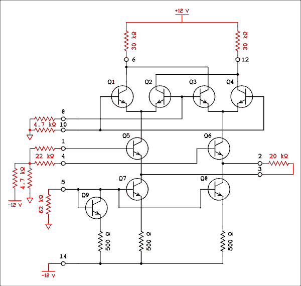
DBMs usually come in the form of an Integrated Circuit (IC) and unlike most ICs the internal circuit is revealed to us mere mortals. The trouble when you see the circuit in an IC manual it is hard to make sense of because the biasing resistors are missing. The designers felt it would be best to allow the design engineer to set the operating point rather than be forced to accept one imposed by the IC manufacturer.In the circuit below I have drawn the internals of the IC in black and the external biasing resistors in red. The setup is the one used in the volume control circuit farther below.
For a verbal description click here.
The current in all the transistors is set by the 62 k ohm resistor connected from pin 5 to ground. Note that pin 14 connects to -12 volts. With such a large resistance the voltage at pin 5 is set by the characteristics of Q9 and the 500 ohm resistor. This voltage is applied to the bases of Q7 and Q8. Because all the transistors were made at the same time under identical conditions they are perfectly matched. The collector currents of Q7 and Q8 are the same as that flowing through the 62 k ohm resistor. This arrangement is often called a current mirror.
Q7 and Q8 are current sinks so the current through Q5 and Q6 is fixed and the sum of the currents in Q1 and Q2, as well as the sum of the currents in Q3 and Q4 is also fixed.
The 20 k ohm resistor connected between pins 2 and 3 allows communication between the emitters of Q5 and Q6. Now the statement can be made that the SUM of the currents in Q5 and Q6 must equal the sum of the currents in Q7 and Q8. The audio signal is applied to the base of Q5. As this signal makes the current in Q5 go up and down the current in Q6 goes down and up. The sum rule makes the currents in Q5 and Q6 to be equal in amplitude and opposite in phase.
You will see that the emitters of Q1 and Q2 are connected together but the collectors of Q1 and Q3 are tied together. That means the alternating current flowing into pin 6 consists of two components of equal amplitude and opposite phase. They cancel out and there is no AC in either pin 6 or pin 12. This is true as long as the currents in Q1, Q2, Q3, and Q4, are all equal.
If the voltage at pin 8 is increased ever so slightly the currents in Q2 and Q3 will increase while an opposite change will take place in Q1 and Q4. This imbalance will result in AC appearing in the resistors connected to pins 6 and 12 and there will be a net output voltage. The two signals at pins 6 and 12 will be equal in amplitude and opposite in phase.
Important to the tone control, but not to the volume control, is if the voltage at pin 8 is made slightly negative the phase of the output signal will be reversed. The farther the voltage at pin 8 is from zero the higher the amplitude of the output.
Normally this circuit is used in radio transmitter and receiver circuits and AC is applied to both input points. (RF is just AC of a higher frequency.) If audio is applied to the lower input and RF is applied to the upper, the output will be double sideband suppressed carrier, if the DC at pins 8 and 10 is balanced. If there is a substantial DC offset applied to 8 and 10 the output will be an AM (amplitude modulated) radio signal. For a further explanation and waveforms take a look at Electrical Fundamentals. AM, SSB, and FM.Voltage Controlled Volume Control.
What we now know as surround sound is really the second incarnation of quadraphonic which had an unsuccessful run in the 70s. In that decade I began construction of a preamp and control center for my sound system. It didn't take me long to find out that 4 ganged pots were just not available. If you see any of the commercial quad equipment from that time you see separate tone and volume controls for front and back channels. I wanted better than that. (Note, a few top end integrated quad amplifiers did use a 4 ganged pot as the volume control.)I designed my control center so all active circuitry was on plug in modules. It looks more like an old mainframe computer than an audio preamp. This has made it easy to alter circuitry I was not happy with. My voltage controlled volume control went through several iterations, this is version 3. The first two used cadmium sulfide photocells. Although they produced low distortion the first version which was open loop with separate tracking adjustments for each channel, 8 in all, had problems with sensitivity to temperature. I added a fifth photocell and went closed loop but tracking became an issue and I knew I had to find another way.
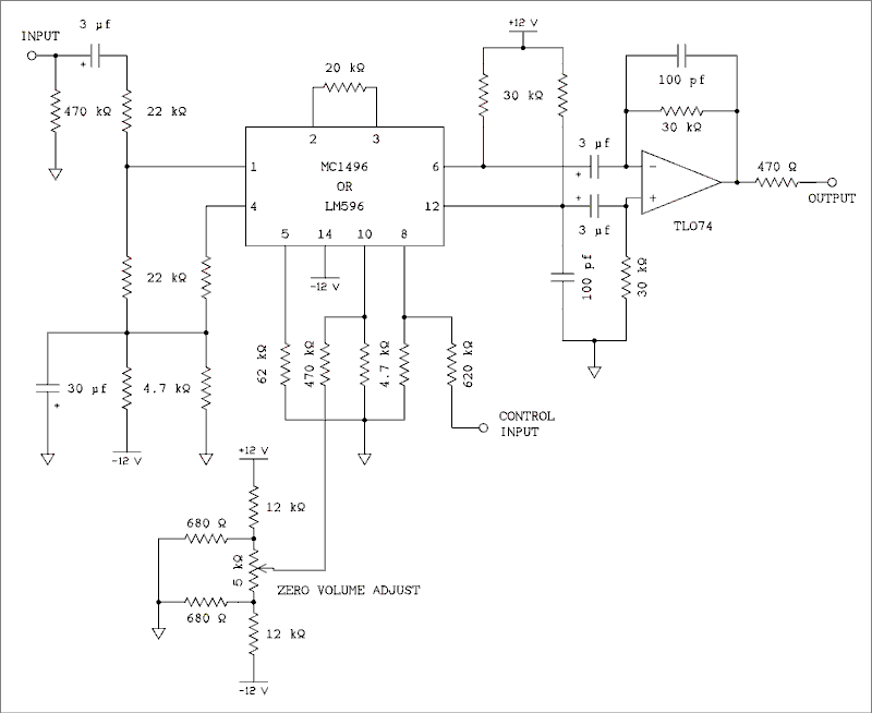
I settled on the DBM based circuit shown below. Actually there are two control boards in the control center. One is the main listening volume control which also incorporates balance controls. The other is in the tape output mostly for doing smooth 4 channel fades. Each board has 4 DBM ICs and one TL074 quad op amp. The tracking is perfect, requiring only a zero volume alignment which I have not had to repeat since finishing these boards in the mid 80s. The circuit was carefully optimized for low distortion and as I remember comes in at about 0.1%.
For a verbal description click here.
The DBM is a linear device so the pot must have an audio taper to give proper volume control performance. Signal is coupled in through a 3 uf capacitor. The extra 22 k ohm resistor is to make sure the DBM will not be overloaded. The differential output of the DBM is coupled by two 3 uf caps to a differential input op amp circuit. This gave much less distortion than single ended coupling.
Of course you don't have to use this circuit as a volume control. You could feed an audio signal to the control voltage input. This will give the ring modulator effect found in early analog synthesizers. The possibilities are limited only by your imagination.
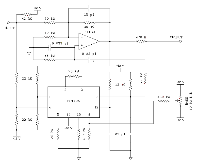
Voltage Controlled Bass Control.
The tone controls like the volume controls above went through several iterations before I got them right. Because I couldn't get 4 ganged pots some kind of electronic control had to be used. I tried one with CdS cells but that wouldn't work well enough to suit me. OTAs were coming along at that time and I gave them a try. The hype from the IC manufacturers touted them as low distortion. Upon reading the fine print I found that their idea of low distortion was anything less than 5%. In reducing the output level to get the distortion to true low levels I ran into the noise floor. The bass control circuit was not too bad because low frequency noise is harder to hear. OTAs in the treble control was out of the question. After a couple of false starts I finally figured out how to make a DBM act like a pot.Below is the schematic of a conventional active tone control using pots.
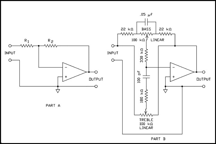
For a verbal description click here.
Notice how the pots connect from the input to the output with the wipers connected to the inverting input of the amplifier block. Because this is an inverting circuit the voltages at each end of one of the pots are opposite in phase and equal in amplitude. When a given pot is set to the exact center of its range the voltage at the wiper is zero. As the wiper is moved off of zero the voltage increases with a given phase and as it is moved off the other way the phase is reversed. Note the similarity with the behavior of the DBM. Each pot in the tone control works this way because of the presence of the other.
For a verbal description click here.
In the circuit above there are two identical resistors, 30 k ohms, to take the place of the other part of the tone control and make the amplifier behave as a unity gain inverting amplifier. The DBM has its inputs, pins 1 and 4, connected between input and output. The 22 k ohm resistors are to properly bias the inputs. Normally the input is driven by the output of another op amp circuit which will hold its voltage at zero. The 43 k ohm resistor to + 12 volts is there to keep the circuit working when it is being operated away from the preamp mainframe.
I took an old DeVry breadboard, mounted an edge connector in it, and fixed it up as a module tester. I can lift any module from the preamp and power it up for testing and trouble shooting. The breadboard was at one time dedicated to module development but when my interest in tubes was renewed I reconverted it for use as a tube breadboard. A photo of it may be seen on the Build a Crystal Set page. To replace the module development part of the DeVry breadboard I mounted two small breadboarding sockets on a plug-in board for module development. That's better anyway because I can test a new module design under actual operating conditions in the preamp.
The 82 pf capacitors from pins 6 and 12 to ground, and the 15 pf cap across the op amp, are to keep things from oscillating at ultrasonic frequencies. Signal is fed from pin 6 of the DBM through an RC network to the noninverting input of the op amp. The 0.82 microfarad cap is only for DC blocking. The 27 k ohm resistor, 68 k ohm resistor, and the 0.033 microfarad capacitor, form a low pass filter permitting only low frequencies to be fed from the DBM to the op amp. Signal is fed to the noninverting input because the inverting input of an op amp has a very low resistance to ground, in fact, almost a dead short. The noninverting input is a high impedance point allowing the RC network to do its job. The 12 k ohm resistor from the inverting input to ground allows signal variations applied to the noninverting input to inject current into the summing node of the op amp. Depending on the phase of the signal fed from the DBM to the noninverting input the signal is either partly canceled, bass cut, or reinforced, bass boost. Because the boost mode is positive feedback it can't be carried too far without the whole thing going into oscillation. It seems to me that 12 or 15 dB was the most I could get and still keep it stable. It's been several years and I can't remember exactly. The amount of boost has proven to be enough. I have never had to turn it up all the way to get the sound I wanted. When the pot is at the center of its range there is no signal through the DBM and the frequency response is flat.
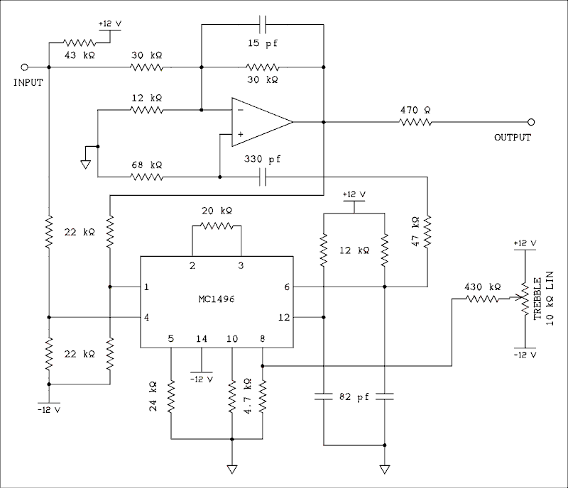
Voltage Controlled Treble Control.
The voltage controlled treble control is almost identical to the bass control. It seems possible that both bass and treble could have been combined into one circuit, although I never tested it. The standard module boards I was using didn't have enough space for both. Each circuit requires 4 DBM ICs along with one quad op amp IC. There just wasn't enough room on one board for 8 DBMs.
Verbal description of the entire circuit.
Verbal description of only what is different from the bass control.
Signal is coupled from the DBM output to the noninverting input of the op amp by the 47 k ohm resistor, the 330 pf capacitor and the 68 k ohm resistor. Together they form a high pass filter allowing only high frequencies to be fed from the DBM output to the op amp input. Depending on the phase of the signal the output signal at the high end will be partially canceled, cut, or reinforced, boosted. When the pot is at the center of its range there is no signal through the DBM and the frequency response is flat.
Magnetic Phono Preamp.
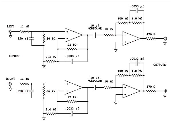
Here is a magnetic phono preamp that unlike most solid state preamps I have had experience with is highly immune to RFI. If you take a map of my area and use a compass to swing a 2 mile radius circle centered on my house, you will include 3 TV transmitters, soon to be 4, 2 FM transmitters, 1 AM transmitter, and the Yellow Cab dispatcher's transmitter. I built this circuit when I grew tired of listening to sync pulse buzz and the programming of the AM station along with my LP records. Tube preamps, for several reasons, are immune to this kind of interference but solid state ones are not. I don't know what equipment manufacturers are doing today but in the 1970s, and earlier, they had not acknowledged that people did live near broadcast transmitters. Note: I started building all of my equipment about 1980 and haven't bought any new audio equipment since. This circuit is one of the plug-in modules in my solid state modularized preamp.
For a verbal description click here.
The 4 op amps are contained in a single TL074 IC. The power supply, not shown, must be very well filtered against 120 cycle hum.
The 11 k ohm resistor in conjunction with the 820 pf capacitor form a low pass filter that does some serious attenuation, 34 dB, on the AM station and really does a number on TV channel 13. This RC combination also works together with the 0.0033 microfarad capacitor and 22 k ohm resistor in the feedback loop to make up the high frequency part of the RIAA curve.
The output of the first op amp and the input of the second one are supposed to be at the same potential but in reality they are not. The problem is, there is no way to predict whether the output of op amp 1 will be positive or negative. The best solution is to use a non-polar electrolytic capacitor for coupling. Failure to use any capacitor here will result in a substantial DC output from the second op amp and a pop when you select phono on the source selector switch.
The RC circuit in the feedback loop of the second op amp makes up the low frequency part of the RIAA curve. The circuit delivers the same level as other sources and sounds good. There's not a trace of AM programming or TV sync pulse buzz.
Headphone Driver.
Here is a very good headphone driver. Each channel employs to of the amplifiers in a TL074 quad op amp, a 2N3904, and a 2N3906. Here is the diagram.
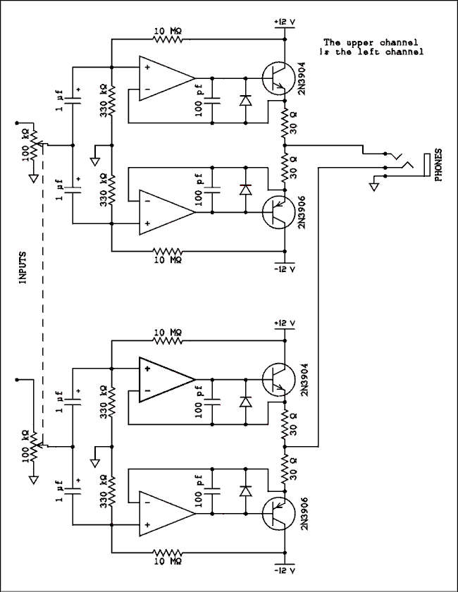
For a verbal description click here.
The circuit uses a complementary pair of small signal transistors as emitter follower drivers. Although I used 2N3904 and 2N3906 you could use almost any other transistors that are of the correct polarity. The TL074 is a FET input amp and serves as an impedance buffer for the bases of the bipolar transistors. The transistors are operating fairly close to ideal class B. The 10 Meg ohm and 330 k ohm resistors serve to bias a little up towards class AB to avoid cross-over distortion. If not for the diodes the op amp on the off side would go to the rail on the opposite side and when called upon to drive the transistor again would have a relatively long recovery time. The combination of the Vbe of the transistor and the forward drop of the diode ensures that the output of the op amp will only be about 1 volt away from driving the base of the transistor. During the short time when the op amp makes the transition from base conduction to diode conduction the loop is momentarily open and it has a tendency to oscillate at RF. The 100 pf capacitor suppresses this oscillation.
If this circuit by itself doesn't provide enough output from your phones you could precede it by one of the gain blocks at the top of this page to obtain the output you desire.
If there are circuits you would like to see on this page drop me a line and I'll see what I can do.
HomeOr use your "Back" button to return to where you were.
This page last updated April 29, 2006.