 n
n
For a verbal description click here.
Building Audio Amplifiers.
200 Watt Per Channel Stereo Amplifier.
High power amplifiers were not my thing but when I realized that music from a CD had a lot more headroom than from any other source I decided it was time to join the power crowd. CDs usually have about 6 dB of headroom and are absolutely linear up to clipping. If you want to reproduce those peaks that the recording companies allow to come just short of clipping you need more power than you did to play vinyl records or tapes.6 dB is 4 times the power so if a 50 watt per channel amplifier was enough for these older media then to play CDs we need 200 watts per channel. That is how this amplifier came into being.
I realize that this line of reasoning is open to more than a little debate but the amplifier was built in the early 90s when my thinking was not quite as clear as it is now.
The Right Way and the Wrong Way.
Back in the tube days there was a saying among audio engineers "There are two ways to design an amplifier, the right way and the wrong way". The right way goes like this. Select the best output transformer you can find for the desired power level or even have one made especially for your company. (If you are going to order several thousand units you can do that). Don't just rely on tube manual data, set up the output tubes and adjust plate, screen and bias voltages for the lowest possible distortion. Design everything carefully for lowest distortion. Add a lot of local feedback to get the distortion even lower. After you have an amplifier which is very clean sounding even without overall feedback add a modest amount, say 20 or 30 dB, to make it even better.The wrong way goes like this. Get the least expensive output transformer you can find, use what ever tubes you can get, slap a phase splitter together and then clean it up with as much feedback as you can cram on it.
What's Wrong with Many Transistor Amplifiers?
Answer: In my opinion, they were designed the wrong way. In the 1960s there was somewhat of a disconnect (generation gap) between the older tube engineers and the young transistor guys. (I came along just at the right time with just the right attitude and took in the knowledge from both groups). The standard transistor power amplifier circuit produces tremendous amounts of distortion 10 or 15 % with the feedback disconnected. The transistor engineers solved the problem, they thought, by cramming on the feedback. Add another stage to get more gain and pour on even more feedback. In Tube amplifiers the phase shift in the output transformer places a practical limit on how much feedback you can put on. There is no such problem with transistor amps. If you are familiar with transistor circuits you will remember that little inductor in the output lead. That's to do a phase correction caused by the transistors at ultrasonic frequencies so they can cram, jam, pack and load on the feedback, as much as 80 dB in some amplifiers I have seen.What's Wrong with That?
Well, it's a matter of delay. To get all that gain they used quite a few transistors. Each transistor has a little time delay. (Tubes have it too). Say a quick transient comes along in the music such as a snare drum or a woodblock. The burst of signal goes through the amplifier and then is returned to the input by the feedback loop. By the time it gets back there part of the transient has already gone. The transient comes out distorted. The trouble with this type of distortion is there is no way to measure it in the laboratory. Distortion tests are made with steady state sine wave tones. Those modern transistor amps come out with distortion figures of 0.0007 % but to the ear they have a harsh sound.Another part of the problem is that the basic circuit of a transistor power amplifier has not changed since the 1960s. I have a GE transistor manual on my book shelf which has the copyright date 1964. It has circuit diagrams of amplifiers ranging in power from 2.5 watts to 15 watts. The transistors have been improved since then, allowing higher power, but the circuit is essentially unchanged. The most prominent features are that the speaker is driven alternately from the emitter of the top transistor and the collector of the bottom one. That's got to cause a lot of distortion. The pre driver has a bootstrapped resistor in its collector. This is actually positive feedback and increases distortion.
By no stretch of the imagination can you say that transistor technology was mature in 1964. Better amplifier circuits could have been designed if any competent engineer had put his mind to it. I designed and built this 200 watt per channel amplifier in the first half of the 90s. I did it the right way using lots of local feedback. The distortion with no overall feedback (none around the complementary outputs) was 0.25 %. After adding 27 dB of feedback I got 0.015. It has an effortless sound.
Hold on a second, doesn't any amount of feedback have the delay problem?
The obvious answer is "yes" but it's a matter of degree. When feedback is used in moderation, the delay effect is not large enough to be audible. The enormous amounts of feedback used in other transistor amps brings the problem up to the level where it is not only audible but objectionable.Some updated information
Maybe my knowledge is a little out of date. That can happen with a retired guy like me. I received an email from a gentleman in Norway who provides this information.I read the article about "What's Wrong with Transistor Amplifiers" and there was mentioned a 10 to 15 percent open loop distortion in transistor amplifiers. There a lot of good amplifiers with no feedback (Counterpoint got less then 0.04% THD). The main problem with adding feedback with transistors has been the performance of the power transistors. The bandwidth of the power transistors in the seventies was so bad and the result was all the problems you mentioned. By combining new quality transistors (Sanken) with moderate local and global feedback loops, new transistor amplifier design has got an excellent performance (Krell, Mark Levinson). The Ft of power transistors has improved from a few hundred kHz to 50 - 80 MHz and that revives the old negative feedback strategies.Thanks for an interesting web site
Old Circuits and Their Problems.
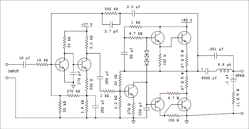
Here is the circuit of the Heathkit AR-15/AA-15. I think it came out in late 1965 or early 1966. The circuit is virtually identical to the circuits in my 1964 GE transistor manual. The only difference is that the voltages, power ratings of the transistors, and output power, are all higher. When you think about it that makes sense. A product may be in development for a year or more before it is brought to the market.I have omitted the current limiting circuit to avoid cluttering the diagram with unnecessary circuitry. The circuit didn't work all that well as I found when I developed a short in my speaker switching box.
n
For a verbal description click here.
The distinguishing features of this circuit are; the inductor in series with the speaker lead, the boot strapped resistors (the 50 uf capacitor going from the amplifier mid point to the junction of the 1 k ohm and 4.7 k ohm resistors), and the fact that the speaker is alternately driven from the emitter of the top power transistor and the collector of the bottom one. This amplifier operates, as most transistor amps do, in deep class B.
There is an argument that says this circuit is really symmetrical and it goes like this. Look at the top output transistor and the one just to its left. The emitter of the left one is connected to the base of the right one and the signal is taken out of the emitter of the right one. This is a circuit known as a Darlington connected emitter follower. Presumably it was invented by someone named Darlington. Note that there are two P-N junctions between the input and the output.
Now look at the lower pair in which a PNP transistor is driving an NPN. Feedback from the collector of the NPN to the emitter of the PNP lowers the overall gain to unity. The DC level on the base of the PNP is one junction away from that on the collector of the NPN. That makes it behave like a Darlington connected emitter follower using two PNP transistors, almost. Note there is one P-N junction between the input and output.
That argument falls apart at high frequencies. The upper Darlington consists of two cascaded emitter followers. What ever voltage you move the base of the input transistor to, the emitter of the second one follows along two P-N junctions behind. Base to collector capacitance isn't any significant problem because it is mostly too small compared to the impedance levels to cause any problem until the frequency gets well up into the RF range. The base to emitter capacitance just helps things along because the signals at the base and emitter are in phase.
In the complementary Darlington, as the bottom circuit is called, the circuit would have a very high gain if it weren't for the feedback from the collector of the NPN to the emitter of the PNP. This is a very large amount of feedback, possibly as much as 40 dB. It's only around two stages so delay is no big problem but phase shift at high frequencies can be. My tests have shown that if it weren't for the 4.7 ohm resistor the circuit would oscillate at around 1 MHz. The amplitude and phase characteristics of the two circuits are different at high frequencies which has to have an effect on the high end of the audio band. Furthermore, the output impedance of the two circuits is different even at low and mid frequencies. The complementary Darlington actually has a lower output impedance than the straight Darlington because of all that feedback.
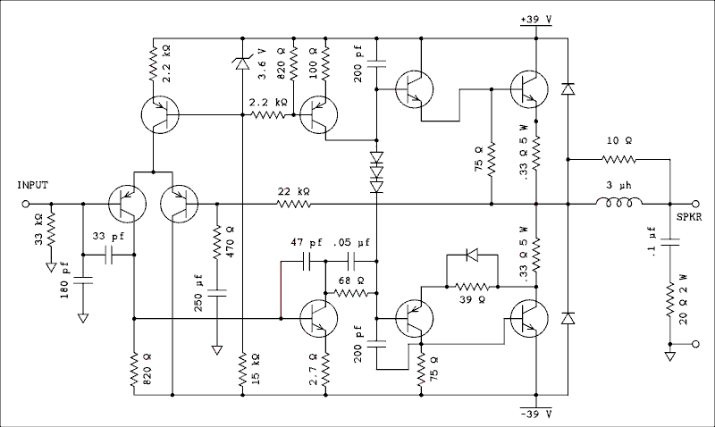
Now, fast forward about 10 years. The Heathkit AA-2015 is a 35 watt per channel 4 channel amplifier. The same circuit, with different transistors and a few changed resistor values was used in the AA-2020 and AR-2020 a 70 watt per channel 2 channel amplifier or receiver.
For a verbal description click here.
The current limiting circuit is quite complex containing two transistors, several diodes, resistors, and capacitors. It was much more effective having been tested by another short, maybe it was the same one, in the same speaker switching box. It has been omitted to keep things simple. After all, this is not a circuit intended for DIY audio.
The bootstrapped resistors have been replaced by a transistor current source. The linearity of transistors does drastically improve when resistive loads are replaced by current sources. The value of the inductor has been more than cut in half which probably says a lot about the high frequency characteristics of the transistors. Coupling to the speaker and through the global feedback loop is now DC. But that damned complementary Darlington is still there.
It did sound a little better than the AR-15 but the use of vary cheap pots on the tone and balance control board was what actually forced me to stop using it. A friend who built an AR-2020 at about the same time I built my AA-2015 has also stopped using his, I suspect for the same reason.
The main problem with both of these amplifiers, as I see it, is the asymmetry of the output circuit. This was done primarily for economics rather than sound engineering. A comparable PNP transistor costs twice as much as its NPN counterpart. That seems like a lot but when you stop and think that power transistors bought in large lots may cost about a dollar each the difference hardly seems worth it in a stereo amplifier costing in excess of 200 dollars. Even Heath was guilty of extreme penny pinching.
My Design.
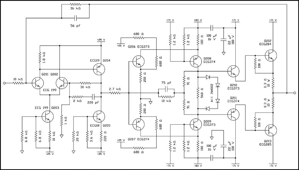
When I started out to build a high quality transistorized amplifier I really didn't know much about how the circuits behaved outside of a global feedback loop. My initial goal was to test the two kinds of power circuits. I have no objection to the complementary Darlington circuit, in fact, I thought using two of them made with complementary transistors would be better than the straight Darlington circuit. But before I could do that I needed a very low distortion driver circuit that would produce the high voltages necessary to drive these circuits.The power amplifier circuits all have unity gain so if I want to apply 40 volts to the load I need a circuit that will give me 40 volts at a very low distortion level. The circuit had to be complementary and completely symmetrical. The four transistor circuit consisting of Q206 through Q209 was what I came up with. The circuit may appear somewhat unorthodox at first viewing because of the two transistor bases that are connected together at the input terminal. This is really a complementary cascode amplifier. Someone looking at the circuit is likely to conclude that I forgot the bypass capacitors on the bases of Q208 and Q209. Not so. Putting bypass capacitors here caused the circuit to oscillate. I think leaving them off is similar to placing a small resistor in series with the base of a wide band amplifier to suppress ringing. The amplifier produced 0.033% distortion at 40 RMS volts output. It seemed natural to use this circuit in the finished amplifier.
To make the output circuit I needed a complementary pair of power transistors 200 V, 200 W, and another complementary pair 200 V, 15 W. The only question was how to hook them up. First I tried an arrangement like the lower transistor in the AR-15. The lower transistor pair was just like the one in the AR-15 while the upper pair consisted of a high power NPN and a medium power PNP. This complementary Darlington connection would not get very close to the positive rail. I'm not sure why, I tried several different transistors of the same type and they all performed about the same.
So next I tried the conventional Darlington connection at both positions. BINGO! I was getting about 0.25% with no global feedback around the output stage. That surprised me because I had always thought that the nonlinearity of the P-N junctions would introduce a lot of distortion. It turns out that the 4 diodes in the driver go a long way towards compensating for this nonlinearity. Notice that they are outside the local feedback loop around the push-pull complementary cascode amplifier circuit.
Notice in the circuits above there were always 3 diodes. The power circuit has 3 P-N junctions between the two drive points. In my amplifier there are 4 P-N junctions between the two drive points of the power circuit, hence there are 4 diodes in the driver. These are usually thought of as being temperature compensation for the idling current but they also do some distortion reduction. Note the 560 ohm resistor between the collectors of Q208 and Q209. Adjusting this resistor would decrease the distortion. If you want to duplicate this circuit and you have distortion measurement equipment you may want to use a rheostat here. The maximum value I found for minimum distortion was 910 ohm and the minimum 560 ohm. The change was small after global feedback was added which is why I used a fixed resistor.
The 56 pf, 75 pf, and 220 pf, capacitors were carefully selected for no ringing square wave response using the ECG or NTE transistors specified. Someone reported building the amplifier and getting oscillation. He may have bypassed the bases of Q208 and Q209. I forgot to ask him in our email exchange.
Don't Blow It.
Don't try a full power test with a 20 kHz sine wave. The outputs will blow before you can adjust your scope.
Don't try a full power square wave test at 10 kHz. Same result.
You can safely do a full power sine wave test up to 10 kHz or square wave up to 1 kHz. You might be able to go a little higher with the square wave but with output pairs going for 10 bucks a pop I really wasn't in the mood to find the exact upper limit.I have been looking through my notebook and I wish I had kept better notes. I guess after I started blowing transistors I became so involved with getting replacements that I neglected to write things down. There is a chart I carefully drew and only one cell is filled in. All this was done a long time ago and I don't remember what I got for the measurements. I constructed the circuits on proto board. It has proven to be too closely spaced and fragile for this much power. What I am saying is the amplifier I built no longer works. Maybe some day I will design a set of PC boards for it and have them made. Until then it sits in my storage building collecting dust.
Listening Tests.
It did work for a while and I had a chance to get used to its sound before the boards started arcing over and blowing transistors. When I first fired it up my immediate impression was of effortless sound. Well, with 200 watts of capability playing at less than a watt that is to be expected. As long as it worked properly I never ran into any source of music that gave any hint of the harshness often associated with other transistor amplifiers I have owned and heard. It would be an interesting experiment to reconstruct it with modern wider band transistors than those used and see how it would measure up. The compensating capacitors would certainly need to be altered to make it stable.Here is the amplifier circuit.
For a verbal description click here.
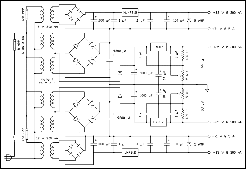
Here is the circuit of the power supply.
For a verbal description click here.