Output Stage Protection
None of my amplifier designs include anything more than a supply line fuse to limit damage from overload and shorted outputs. Speaker protection in the form of an output coupling capacitor is included in all my recent designs, and even in the event of capacitor failure the overall feedback still limits the maximum speaker voltage. Speakers can be very expensive to repair, and excessive heatsink temperature can be dangerous, so a 70deg.C thermal cutout attached to the heatsink is strongly recommended.
Protection of the amplifier output stage against shorted or excessively low impedance load is less essential. I try to avoid connecting my amplifiers to any load unless I am entirely certain it is safe to do so, and I suggest that for most DIY constructors the time taken to ensure such safety is far less than the time taken to design or build protection circuits. The use of well insulated 'figure-8' speaker cables may be safer than some of the high capacitance types with low separation between conductors. Mistakes do happen of course, but it could be argued that shorting our amplifier output and watching the smoke drifting upwards is a valuable learning experience, and the cost of replacing a few power transistors will encourage us to be more careful next time. For commercial or professional use the omission of protection is generally not an acceptable option.
Some modern high power transistors are actually quite difficult to destroy, and a simple 3A supply line fuse in one case came to the rescue during testing when I foolishly applied a 100kHz full power square wave to a 4uF capacitor load. This is not something I would recommend anyone try, they may not be so lucky. The supply line fuses are essential, otherwise there is little to limit the supply or output current under fault conditions, and although occasional stories about speaker cables bursting into flame with shorted loads seem highly unlikely this sort of risk must certainly be avoided. The 2A fuse together with the use of lateral mosfets in my latest designs makes damage even less likely.
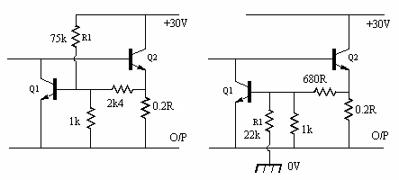
If load-line protection is to be included there are simple and well known ways to do this. The simplest, giving just a straight-line approximation to the output transistor safe operating area (SOA) is shown below on the left for one half of a class-B direct coupled output stage using plus and minus 30V supplies:
Shown here as a single transistor, Q2 is normally a darlington or cfp. There are two small problems with this circuit, one is that supply line noise is injected into the circuit via R1, and also the protection transistor is already biased on slightly even with no amplifier output voltage or current, with as much as 300mV base-emitter voltage. In practice neither 'problem' is likely to be serious, but both can be solved or at least improved just by taking R1 to earth (0V) instead of the positive supply, as in the second circuit. The resistor values need to be recalculated, and some very approximate values are shown for the load line example used later. One disadvantage is that the supply voltage needs to be known to calculate correct values, so variations of the supply voltage are a slightly greater problem. The base-emitter voltage of the protection transistor now varies from -600mV to +600mV instead of the 0mV to +600mV of the first version, and is close to zero for zero amplifier output, so any tendency for the transistor to conduct at high signal levels and thereby add distortion should be reduced. In practice for either circuit a diode in series with the collector may be needed to prevent reverse bias on the protection transistor, and also various resistors and diodes can be added to give a closer match to the safe operating area of the output transistor.
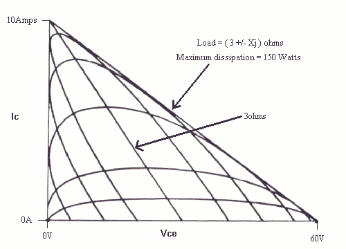
If the maximum possible power output is to be permitted before limiting occurs a more complex circuit is needed. Looking at published versions it is a little surprising that there is rarely any attempt to match anything more than the dc safe operating region of the power transistors at a fixed temperature. Circuits allowing increased dissipation for shorter time periods are hard to find, while reducing maximum dissipation as case temperature rises seems almost unheard of, although temperature derating is invariably included in transistor data sheets. To see why this could be important consider the load lines for an amplifier with a 60V supply designed to drive 3ohm speakers. If 3ohms is the dc resistance for a simple single moving coil driver then there will be additional reactive impedance components at different frequencies, and for a range of values of the reactance the load lines are as shown next:
A worse case would be if the lowest impedance and highest phase angle occurred at the same frequency, but even for a more complex speaker with several drive units and crossover network this appears not to be the case. Looking at a few published graphs of speaker impedance shows that the minimum impedances invariably occur at the frequencies where the phase angle is close to zero, i.e. the impedance is resistive. (It is also resistive when the impedance is a maximum.) I am not certain how accurate this is or whether there are exceptions to the rule, though I have a vague memory that it is only strictly correct for 'minimum phase' networks, which speakers are not because of time delay effects involving reflected acoustic energy.
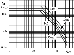
The SOA of a typical transistor, rated at 200watts, which we could choose for this amplifier is shown next:
Comparing the voltages and currents it can be seen that the load lines fit easily within the dc SOA of the transistor, so there should be no problem. Unfortunately the thermal derating mentioned earlier changes this result. This particular device is derated from 200watts down to 135watts with its case temperature at 70deg.C, and the load line passing through 30V and 5Amps gives peak dissipation 150 watts, so the safe operating area is exceeded. (The maximum current should probably also be derated, though this is mentioned less often in data sheets). The maximum power is only exceeded by about 11%, and this is unlikely to happen at very low frequencies, so the 100msec SOA can be assumed to be applicable, and destruction is highly unlikely. (Actually we should use a derating based on heatsink temperature rather than case temperature because our 70deg thermal cutout will be attached to the heatsink, so case temperature can be higher.) Had we constructed some sort of protection circuit operating within the derated dc SOA however this would operate and cause heavy distortion. Including both temperature and time compensation however the protection would not operate, while at lower case temperatures higher short-term power into lower impedance loads would be possible. The added complexity compared to typical protection circuits need be little more than an extra capacitor and resistor, plus thermal contact between the protection circuit transistor and the heatsink. Resistor values need to be recalculated, it is not enough just to take an existing protection circuit and add thermal contact between protection transistors and heatsink, as shown in the next section.
Temperature Compensation.
To confirm that the thermal coupling suggested would give something reasonably close to the required derating the initial calculation I did assumed a conventional circuit rather than the 'improved' version I suggested, with 300mV Vbe for the sensor transistor with no amplifier output, and 600mV needed to switch it on at 20deg C. At higher temperature this 600mV will reduce by about 2mV per deg, so it will fall to 300mV at about 170deg, and so the sensor transistor will switch on even with no signal and prevent further dissipation in the power device when 170deg is reached. Looking at power transistor derating specifications the case temperature at which they are derated to zero seems to vary between 150 and 200deg, so we are in the right area. Hopefully the heatsink temperature will be limited to something like 70deg by a thermal cutout, but the derating is a linear function of temperature, so if it is about right at 170 deg it should be fairly close at 70 also. In practice there are other factors to take into account, such as the difference between the power transistor case temperature and the sensor transistor junction temperature.
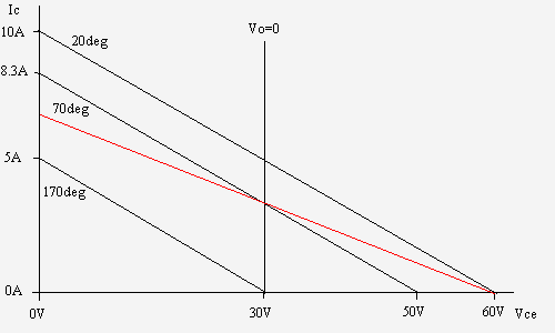
A bigger problem is that the straight line approximation to constant power is already inaccurate, and changing the sensor temperature makes it even worse. What we really need is for the sensor transistor to have Vbe = 300mV + kVI, where k is some constant and V and I are the collector-emitter voltage and current of the power transistor. What we have in the standard circuit is Vbe = aV + bI where a and b are constants. The next diagram shows what happens if we design for the best straight line at 20deg, and then use thermal coupling to reduce the maximum power at higher temperatures. Supply voltages of plus and minus 30V are again used.
At 170deg the power is reduced to zero at zero output voltage, corresponding to 30V power transistor voltage, but a current of several amps is still theoretically possible at reduced voltage. In practice we would hope the temperature could never reach 170deg, and the suggested 70deg thermal cutout will prevent this. More serious is the reduction of output current to zero at 70deg before reaching the maximum output voltage into reactive loads. A better result would be the line shown in red, but this is not so easy to achieve in practice.
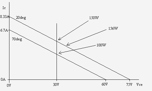
A better alternative is to design for the best straight line approximation at the derated power at 70deg, and this result is shown next:
The 70deg line is what we would have to use if no thermal coupling was used and we wanted to keep the power transistors within their safe operating area up to 70deg. With the thermal coupling there is now at 20deg an extra 50% current available at Vo = 0, plus 24% greater peak current into low resistive loads. The higher current at higher voltages will help with highly reactive loads. The only negative effect is that the maximum power reaches 156W, slightly over the 150W limit, but not enough to worry about.
The same approach could be tried for more complex circuits designed to increase permitted current at high and low voltages to give a better approximation to constant power. (e.g. see Becker, 'High-power Audio Amplifier Design', Wireless World, Feb 1972, p81.) Designing for optimum results at 70deg with thermal coupling will give improved maximum output current at lower temperature, but the result for the single line approximation suggests that care may then be needed to avoid allowing the maximum power limit to be exceeded.
The calculation in the first paragraph assumed a 2mV per deg.C fall in Vbe, but looking at data sheets for a more accurate value I found that for any given transistor the value is a function of collector current. For example the BC546 is specified as 2mV/deg.C at Ic=5mA, 2.2mV/deg.C at Ic=1mA and 1.8mV/deg.C at Ic=20mA. To add further complication the value is different for other transistor types. The currents at which Vbe falls by 2mV per deg.C are 10mA for a BC486, 20mA for a BC485, and 40mA for a MPSA05. These figures are taken from Motorola data sheets, and there is no certainty that the same types from other manufacturers will have identical specifications. It is also not clear how far the values can vary between samples, the figures appear to be only 'typical'. It is fortunate that exact figures are not essential, and even approximate compensation can give a worthwhile increase in available output at low temperatures.
If the sensor transistor is not in thermal contact with the heatsink then there is some difficulty knowing what temperature it will be operating at. A board mounted component will be at a virtually unpredictable temperature depending on distance from heatsink, ventilation of the case, room temperature, and also with various thermal time constants involved. So how can the value of Vbe at which the sensor transistor conducts be determined? Thermal contact with the heatsink I suggest is not only a good way to increase available output at low temperatures, but also a more predictable way to add SOA protection.
The use of protection circuits to sense voltage, current, case temperature, and time duration are just an attempt to predict the junction temperature and to prevent it exceeding its maximum value, typically 170 deg.C, but achieving a high level of accuracy is difficult. A far simpler method would be to detect the junction temperature directly, and reduce the power dissipation only when the 170 deg limit is approached. This appears to be the method used in some National Semiconductor integrated circuit power amplifiers such as the LM1876 and LM4766. There are power transistors available (the SAP15N darlington for example) with built in temperature sensor diodes, but these appear to be only intended for stabilising quiescent current, and I am not sure whether they could also be used effectively in a protection circuit.
Turning down the volume control is all we need do to avoid the simplest straight line protection circuit operating with low load impedance. The only reason to use more complex protection is to get closer to the maximum possible power output of the transistors chosen, but a just audible 1dB increase needs a 26% increase in power, so any improvement needs to be greater than this to have any real value.
HOME.