BUILDING THE MJR7-Mk5. PHOTOS

The photos are of what was intended to be the final MJR7-Mk5. I forgot that the resistors I had previously planned to use were 0.25W and the ones I ordered are 0.5W. The board was designed for the smaller size resistors, and fitting the larger size the leads had to be bent very close to the resistor body in some cases. The first photo shows the resistors fitted, and it can be seen that there are a few different sizes. Most are the 0.5W types, there are only two 0.25W and also two 0.125W. I have done a few adjustments to the board design, and the 0.5W should now fit easier than in this photo. A few other small adjustments were made, for example the input terminal block is now slightly further forward than in the photo to give more space for the 560k resistors, which still need to be the very small 0.125W types. I have also increased the space round the 63V electrolytics so that larger 100V types could be used. The 4700u should now be ok up to 30mm diameter, and the 470u up to 16mm, but then it may be a good idea to fit the components close to the electrolytics only when the capacitors are in place to be sure there is no obstruction.

The spacers used to fix the board to a base are shown next. One of these is the star earth point, and to ensure a good connection from the board to the case I used a solder tag instead of the washers used on the other two spacers, with the tag soldered to the earth track on the board. I only used a single bolt through the case to hold the board in place, the other two spacers just rest on the base to support the weight of the board.

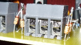
The terminal blocks should be fitted before the 300R or 560k resistors so that the resistors can be routed not to obstruct the blocks. As shown next there is minimal clearance, and if the resistors are added first the blocks may not be easy to fit. The 560k clearance has since been improved a little.


Next the capacitors and inductors are added:


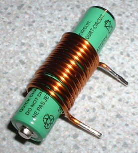
One of the inductors is shown next. It is air-cored, and is made using 18-gauge enamelled copper wire (1.2mm dia.) which can be made by winding it on a 1cm dia former, for example an AAA battery as shown in the photo. There are 13 turns, giving an overall length about 17mm. The other photo shows how the gate protection zeners are fitted. To save space only two holes are provided and the zeners have two ends soldered together off the board. The connected ends are the same polarity, in the photo the cathodes (indicated by a dark band) are connected, but it works just the same if anodes are connected together instead. Don't try using a normal diode in series with a zener, that works in some mosfet circuits, but not in this one.
Next the on-board transistors and diodes are added. The 2SC2911 transistors have their collector pins bent out to reach over an earth track as shown first. The layout could have been neater, but using a single sided board and avoiding the need for wire links was considered more important.
Next the board is attached to the base plate and mosfets with heatsink, and wired up for testing.
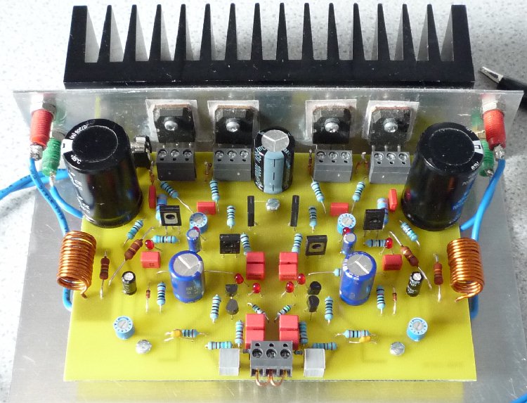

The connections under the board are just two wires to the power supply plus the two pairs of speaker wires. This board was 'tinned' with out of date tinplate solution, which is why it looks more copper coloured. The tinning chemical has a limited shelf life once mixed with water, I need to order some more for the first batch of boards.